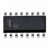
MC74HC595ADG ON Semiconductor, MC74HC595ADG Datasheet - Page 6

MC74HC595ADG
Manufacturer Part Number
MC74HC595ADG
Description
IC SHIFT REGISTER 8BIT 16-SOIC
Manufacturer
ON Semiconductor
Series
74HCr
Datasheet
1.MC74HC595ANG.pdf
(11 pages)
Specifications of MC74HC595ADG
Logic Type
Shift Register
Output Type
Standard
Number Of Elements
1
Number Of Bits Per Element
8
Function
Serial to Parallel
Voltage - Supply
2 V ~ 6 V
Operating Temperature
-55°C ~ 125°C
Mounting Type
Surface Mount
Package / Case
16-SOIC (3.9mm Width)
Counting Sequence
Serial to Serial/Parallel
Number Of Circuits
2
Logic Family
74HC
Propagation Delay Time
140 ns, 100 ns, 28 ns, 24 ns
Supply Voltage (max)
6 V
Maximum Operating Temperature
+ 125 C
Minimum Operating Temperature
- 55 C
Mounting Style
SMD/SMT
Operating Supply Voltage
2 V to 6 V
Lead Free Status / RoHS Status
Lead free / RoHS Compliant
Other names
MC74HC595ADG
MC74HC595ADGOS
MC74HC595ADGOS
Available stocks
Company
Part Number
Manufacturer
Quantity
Price
SR = shift register contents
LR = latch register contents
INPUTS
A (Pin 14)
8−bit serial shift register.
CONTROL INPUTS
Shift Clock (Pin 11)
this input causes the data at the Serial Input pin to be shifted
into the 8−bit shift register.
Reset (Pin 10)
low on this pin resets the shift register portion of this device
only. The 8−bit latch is not affected.
Latch Clock (Pin 12)
this input latches the shift register data.
Reset shift register
Shift data into shift
register
Shift register remains
unchanged
Transfer shift register
contents to latch
register
Latch register remains
unchanged
Enable parallel outputs
Force outputs into high
impedance state
Serial Data Input. The data on this pin is shifted into the
Shift Register Clock Input. A low− to−high transition on
Active−low, Asynchronous, Shift Register Reset Input. A
Storage Latch Clock Input. A low−to−high transition on
Operation
Reset
H
H
H
X
X
X
L
D = data (L, H) logic level
U = remains unchanged
Serial
Input
A
X
D
X
X
X
X
X
L, H, ↓
L, H, ↓
Clock
Inputs
Shift
X
↑
X
X
X
PIN DESCRIPTIONS
L, H, ↓
L, H, ↓
L, H, ↓
L, H, ↓
http://onsemi.com
FUNCTION TABLE
Clock
Latch
X
X
↑
↑ = Low−to−High
↓ = High−to−Low
Output
Enable
6
H
L
L
L
L
L
L
Output Enable (Pin 13)
data from the latches to be presented at the outputs. A high
on this input forces the outputs (Q
high−impedance state. The serial output is not affected by
this control unit.
OUTPUTS
Q
SQ
eighth stage of the 8−bit shift register. This output does not
have three−state capability.
A
Active−low Output Enable. A low on this input allows the
Noninverted, 3−state, latch outputs.
Noninverted, Serial Data Output. This is the output of the
H
− Q
SR
(Pin 9)
Contents
D → SR
H
Register
N
(Pins 15, 1, 2, 3, 4, 5, 6, 7)
Shift
→ SR
U
U
L
*
*
*
A
N+1
;
* = depends on Reset and Shift Clock inputs
** = depends on Latch Clock input
SR
Resulting Function
Contents
Register
Latch
N
→ LR
U
U
U
U
**
**
N
SR
Output
Serial
G
SQ
→ SR
U
U
L
*
*
*
H
A
−Q
H
H
) into the
Outputs
Q
Parallel
Enabled
A
SR
U
U
U
U
Z
− Q
N
H


