MC74HC139ANG ON Semiconductor, MC74HC139ANG Datasheet
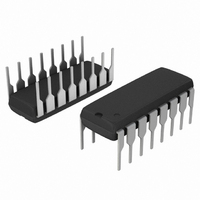
IC DECODER/DEMUX DUAL 1-4 16DIP

MC74HC139ANG

Manufacturer Part Number
MC74HC139ANG
Description
IC DECODER/DEMUX DUAL 1-4 16DIP
Manufacturer
ON Semiconductor
Series
74HCr
Type
Decoder/Demultiplexerr
Datasheet

Specifications of MC74HC139ANG

Circuit
1 x 2:4
Independent Circuits
2
Current - Output High, Low
5.2mA, 5.2mA
Voltage Supply Source
Single Supply
Voltage - Supply
2 V ~ 6 V
Operating Temperature
-55°C ~ 125°C
Mounting Type
Through Hole
Package / Case
16-DIP (0.300", 7.62mm)
Product
Decoders, Encoders, Multiplexers & Demultiplexers
Logic Family
74HC
Number Of Bits
2
Number Of Lines (input / Output)
1.0 / 4.0
Supply Voltage (max)
6 V
Supply Voltage (min)
2 V
Maximum Operating Temperature
+ 125 C
Minimum Operating Temperature
- 55 C
Mounting Style
SMD/SMT
Number Of Input Lines
1.0
Number Of Output Lines
4.0
Logic Type
Decoder / Demultiplexer
No. Of Outputs
4
Supply Voltage Range
2V To 6V
Logic Case Style
DIP
No. Of Pins
16
Operating Temperature Range
-55°C To +125°C
Filter Terminals
DIP
Rohs Compliant
Yes
Family Type
HC
Lead Free Status / RoHS Status
Lead free / RoHS Compliant
Other names
MC74HC139ANGOS
MC74HC139A
Dual 1−of−4 Decoder/
Demultiplexer
High−Performance Silicon−Gate CMOS
inputs are compatible with standard CMOS outputs; with pull−up
resistors, they are compatible with LSTTL outputs.
which decodes a two−bit Address to one−of−four active−low outputs.
Active−low Selects are provided to facilitate the demultiplexing and
cascading functions. The demultiplexing function is accomplished by
using the Address inputs to select the desired device output, and
utilizing the Select as a data input.
Features
*For additional information on our Pb−Free strategy and soldering details, please
© Semiconductor Components Industries, LLC, 2005
June, 2005 − Rev. 9
download the ON Semiconductor Soldering and Mounting Techniques
Reference Manual, SOLDERRM/D.
The MC74HC139A is identical in pinout to the LS139. The device
This device consists of two independent 1−of−4 decoders, each of
No. 7A
Output Drive Capability: 10 LSTTL Loads
Outputs Directly Interface to CMOS, NMOS and TTL
Operating Voltage Range: 2.0 to 6.0 V
Low Input Current: 1.0 mA
High Noise Immunity Characteristic of CMOS Devices
In Compliance with the Requirements Defined by JEDEC Standard
Chip Complexity: 100 FETs or 25 Equivalent Gates
Pb−Free Packages are Available*
1
16
16
See detailed ordering and shipping information in the package
dimensions section on page 2 of this data sheet.
16
16
1
1
1
1
ORDERING INFORMATION
A
L, WL
Y, YY
W, WW
G
G
(Note: Microdot may be in either location)
http://onsemi.com
CASE 751B
CASE 948F
SOEIAJ−16
TSSOP−16
DT SUFFIX
CASE 648
CASE 966
N SUFFIX
D SUFFIX
F SUFFIX
PDIP−16
SOIC−16
= Assembly Location
= Wafer Lot
= Year
= Work Week
= Pb−Free Package
= Pb−Free Package
Publication Order Number:
16
16
1
1
16
1
MC74HC139AN
MC74HC139A/D
DIAGRAMS
AWLYYWWG
16
1
MARKING
HC139AG
AWLYWW
74HC139A
ALYWG
ALYWG
139A
HC
G

Related parts for MC74HC139ANG

MC74HC139ANG Summary of contents

Page 1

... Chip Complexity: 100 FETs or 25 Equivalent Gates • Pb−Free Packages are Available* *For additional information on our Pb−Free strategy and soldering details, please download the ON Semiconductor Soldering and Mounting Techniques Reference Manual, SOLDERRM/D. © Semiconductor Components Industries, LLC, 2005 June, 2005 − Rev. 9 http://onsemi.com PDIP− ...

Page 2

... don’t care ORDERING INFORMATION Device MC74HC139AN MC74HC139ANG MC74HC139AD MC74HC139ADG MC74HC139ADR2 MC74HC139ADR2G MC74HC139ADTR2 MC74HC139ADTR2G MC74HC139AFEL MC74HC139AFELG †For information on tape and reel specifications, including part orientation and tape sizes, please refer to our Tape and Reel Packaging Specifications Brochure, BRD8011/D. *This package is inherently Pb−Free. ...

Page 3

... Tested to EIA/JESD22−A114−A. 3. Tested to EIA/JESD22−A115−A. 4. Tested to JESD22−C101−A. 5. Tested to EIA/JESD78. 6. For high frequency or heavy load considerations, see Chapter 2the ON Semiconductor High−Speed CMOS Data Book (DL129/D). RECOMMENDED OPERATING CONDITIONS Symbol Î Î Î Î Î Î Î Î Î Î Î Î Î Î Î Î Î Î Î Î Î Î Î Î Î ...

Page 4

... For propagation delays with loads other than 50 pF, and information on typical parametric values, see the ON Semiconductor High−Speed CMOS Data Book (DL129/D). ...

Page 5

SELECT 10% t PHL 90% 50% OUTPUT Y 10% t THL Figure 3. Switching Waveform MC74HC139A INPUT A GND t PLH t PLH OUTPUT Y t TLH Figure 4. Switching Waveform TEST ...

Page 6

ADDRESS INPUTS (Pins 2, 3, 14, 13 Address inputs. These inputs, when the respective 1−of−4 decoder is enabled, determine which of its four active−low outputs is selected. CONTROL INPUTS ...

Page 7

0.25 (0.010) M −A− −T− SEATING PLANE 0.25 (0.010 MC74HC139A PACKAGE DIMENSIONS PDIP−16 ...

Page 8

K 16X REF 0.10 (0.004) 0.15 (0.006 L PIN 1 IDENT. 1 0.15 (0.006 −V− C 0.10 (0.004) SEATING −T− D PLANE MC74HC139A PACKAGE DIMENSIONS TSSOP−16 DT SUFFIX CASE 948F−01 ...

Page 9

VIEW 0.10 (0.004) 0.13 (0.005) M MC74HC139A PACKAGE DIMENSIONS SOEIAJ−16 F SUFFIX CASE 966−01 ISSUE O NOTES DETAIL ...

Page 10

... Fax: 480−829−7709 or 800−344−3867 Toll Free USA/Canada Email: orderlit@onsemi.com MC74HC139A N. American Technical Support: 800−282−9855 Toll Free USA/Canada Japan: ON Semiconductor, Japan Customer Focus Center 2−9−1 Kamimeguro, Meguro−ku, Tokyo, Japan 153−0051 Phone: 81−3−5773−3850 http://onsemi.com 10 ON Semiconductor Website: http://onsemi ...

Related keywords