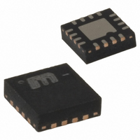
SY89840UMG TR Micrel Inc, SY89840UMG TR Datasheet

SY89840UMG TR
Specifications of SY89840UMG TR
SY89840UMGTR
Related parts for SY89840UMG TR
SY89840UMG TR Summary of contents
Page 1
... All support documentation can be found on Micrel’s web site at: www.micrel.com. Precision Edge is a registered trademark of Micrel, Inc. Micrel Inc. • 2180 Fortune Drive • San Jose, CA 95131 • USA • tel +1 (408) 944-0800 • fax + 1 (408) 474-1000 • http://www.micrel.com February 2005 SY89840U ...
Page 2
Typical Application February 2005 Simplified Example Illustrating RPE (Runt Pulse Elimination) Circuit when Primary Clock Fails 2 hbwhelp@micrel.com M9999-021705 or (408) 955-1690 ...
Page 3
Ordering Information Part Number Package Type SY89840UMG (2) SY89840UMGTR Notes: 1. Contact factory for die availability. Dice are guaranteed Tape and Reel. Pin Configuration February 2005 Operating Range QFN-16 Industrial QFN-16 Industrial = 25°C, DC Electricals ...
Page 4
Pin Description Pin Number Pin Name 4, 1, IN0, /IN0, 16, 13 IN1, /IN1 3, 15 VT0, VT1 VREF-AC0 2, 14 VREF-AC1 10 SEL VCC GND 9 Exposed Pad 11 CAP Truth Table ...
Page 5
Micrel, Inc. Absolute Maximum Ratings Supply Voltage (V ) .............................................. –0.5V to +4.0V CC Input Voltage (V ) ......................................................–0. LVPECL Output Current (I ) OUT Continuous ......................................................... ±50mA Surge................................................................ ±100mA Termination Current Source/Sink Current on V ........................................ ...
Page 6
LVPECL Outputs DC Electrical Characteristics V = 2.5V ±5% or 3.3V ±10 Symbol Parameter V Output HIGH Voltage Output Low Voltage Output Voltage Swing OUT Differential Output ...
Page 7
AC Electrical Characteristics V = 2.5V ±5% or 3.3V ±10 Symbol Parameter f Maximum Operating Frequency MAX t Differential Propagation Delay In-to Differential Propagation Delay pd Tempco Temperature Coefficient t Part-to-Part Skew SKEW t Jitter Cycle-to-Cycle ...
Page 8
Functional Description RPE MUX and Fail-Safe Input The SY89840U is optimized for clock switchover applications where switching from one clock to another clock without runt pulses (short cycles) is required. It features two unique circuits: Runt-Pulse Eliminator (RPE) Circuit: The ...
Page 9
Case #2 Input Clock Failure: Switching from a selected clock stuck HIGH to a valid clock (RPE enabled). If CLK1 fails HIGH before the RPE MUX selects CLK2 (using the SEL pin), the switchover will occur in three stages. Note: ...
Page 10
Case #4 Input Clock Failure: Switching from the selected clock input stuck in an undetermined state to a valid clock input (RPE enabled). If CLK1 fails to an undetermined state (e.g., amplitude falls below the 100mV (V single-ended input limit, ...
Page 11
Typical Operating Characteristics V = 3.3V, GND = 0V, V ≥ 400mV CC IN February 2005 , t /t ≤ 300ps 50Ω –2V 25°C, unless otherwise stated. A ...
Page 12
Singled-Ended and Differential Swings Figure 1a. Single-Ended Voltage Swing Input and Output Stages Figure 2a. Simplified Differential Input Stage February 2005 Figure 1b. Differential Voltage Swing Figure 2b. Simplified LVPECL Output Stage 12 hbwhelp@micrel.com M9999-021705 or (408) 955-1690 ...
Page 13
Input Interface Applications Figure 3a. LVPECL Interface (DC-Coupled) Figure 3d. CML Interface (AC-Coupled) February 2005 Figure 3b. LVPECL Interface (AC-Coupled) Figure 3e. LVDS Interface 13 Option: may connect Figure 3c. CML Interface (DC-Coupled) M9999-021705 hbwhelp@micrel.com ...
Page 14
LVPECL Output Interface Applications LVPECL has a high input impedance, a very low output impedance (open emitter), and a small signal swing which results in low EMI. LVPECL is ideal for driving 50Ω and 100Ω controlled impedance transmission lines. There ...
Page 15
QFN - 16 MICREL, INC. 2180 FORTUNE DRIVE SAN JOSE, CA 95131 USA TEL +1 (408) 944-0800 FAX +1 (408) 474-1000 WEB http:/www.micrel.com The information furnished by Micrel in this data sheet is believed to be accurate and reliable. However, ...


