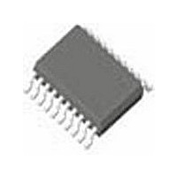
PI5C3245LE Pericom Semiconductor, PI5C3245LE Datasheet - Page 2

PI5C3245LE
Manufacturer Part Number
PI5C3245LE
Description
IC 8-BIT BUS SW 2-PORT 20-TSSOP
Manufacturer
Pericom Semiconductor
Type
Bus Switchr
Datasheet
1.PI5C3245QE.pdf
(5 pages)
Specifications of PI5C3245LE
Circuit
8 x 1:1
Independent Circuits
1
Voltage Supply Source
Single Supply
Voltage - Supply
4 V ~ 5.5 V
Operating Temperature
-40°C ~ 85°C
Mounting Type
Surface Mount
Package / Case
20-TSSOP
Number Of Bits
8
Number Of Elements
1
Technology
CMOS
High Level Output Current
-120mA
Low Level Output Current
120mA
On Resistance
10Ohm
Propagation Delay Time
6.5ns
Package Type
TSSOP
Operating Temp Range
-40C to 85C
Operating Temperature Classification
Industrial
Operating Supply Voltage (min)
4.75V
Operating Supply Voltage (typ)
5V
Operating Supply Voltage (max)
5.25V
Quiescent Current
3uA
Pin Count
20
Mounting
Surface Mount
Lead Free Status / RoHS Status
Lead free / RoHS Compliant
Current - Output High, Low
-
Lead Free Status / RoHS Status
Lead free / RoHS Compliant, Compliant
Available stocks
Company
Part Number
Manufacturer
Quantity
Price
1 2 3 4 5 6 7 8 9 0 1 2 3 4 5 6 7 8 9 0 1 2 3 4 5 6 7 8 9 0 1 2 1 2 3 4 5 6 7 8 9 0 1 2 3 4 5 6 7 8 9 0 1 2 3 4 5 6 7 8 9 0 1 2 1 2 3 4 5 6 7 8 9 0 1 2 3 4 5 6 7 8 9 0 1 2 3 4 5 6 7 8 9 0 1 2 1 2 3 4 5 6 7 8 9 0 1 2 3 4 5 6 7 8 9 0 1 2 3 4 5 6 7 8 9 0 1 2 1 2 3 4 5 6 7 8 9 0 1 2
1 2 3 4 5 6 7 8 9 0 1 2 3 4 5 6 7 8 9 0 1 2 3 4 5 6 7 8 9 0 1 2 1 2 3 4 5 6 7 8 9 0 1 2 3 4 5 6 7 8 9 0 1 2 3 4 5 6 7 8 9 0 1 2 1 2 3 4 5 6 7 8 9 0 1 2 3 4 5 6 7 8 9 0 1 2 3 4 5 6 7 8 9 0 1 2 1 2 3 4 5 6 7 8 9 0 1 2 3 4 5 6 7 8 9 0 1 2 3 4 5 6 7 8 9 0 1 2 1 2 3 4 5 6 7 8 9 0 1 2
Notes:
1. For Max. or Min. conditions, use appropriate value specified under Electrical Characteristics for the applicable device type.
2. Typical values are at V
3. Not more than one output should be shorted at one time. Duration of the test should not exceed one second.
4. Measured by the voltage drop between A and B pin at indicated current through the switch. ON resistance is determined by the lower of the
Capacitance
Notes:
1. This parameter is determined by device characterization but is not production tested.
DC Electrical Characteristics
Parameters
Parameters Description
Maximum Ratings
(Above which the useful life may be impaired. For user guidelines, not tested.)
Storage Temperature ................................................................. –65°C to +150°C
Ambient Temperature with Power Applied ................................ –40°C to +85°C
Supply Voltage to Ground Potential (Inputs & Vcc Only) .......... –0.5V to +7.0V
Supply Voltage to Ground Potential (Outputs & D/O Only) ....... –0.5V to +7.0V
DC Input Voltage ......................................................................... –0.5V to +7.0V
DC Output Current ................................................................................... 120 mA
Power Dissipation ......................................................................................... 0.5W
voltages on the two (A,B) pins.
C
C
C
V
V
I
I
I
V
I
V
R
IH
IL
OS
IN
OFF
ON
OZH
IH
IL
IK
H
ON
06-0239
(1)
Input HIGH Voltage
Input LOW Voltage
Input HIGH Current
Input LOW Current
High Impedance Output Current
Clamp Diode Voltage
Short Circuit Current
Input Hysteresis at Control Pins
Switch On Resistance
(T
A
= 25°C, f = 1 MHz)
Description
Input Capacitance
A/B Capacitance, Switch Off
A/B Capacitance, Switch On
CC
= 5.0V, T
A
(3)
= 25°C ambient and maximum loading.
(4)
(Over the Operating Range, T
Guaranteed Logic HIGH Level
Guaranteed Logic LOW Level
V
0 ≤A, B ≤V
A (B) = 0V, B (A) = V
V
V
V
V
CC
CC
CC
CC
CC
Test Conditions
= Max., V
= Max., V
= Min., I
= Min., V
= Min., V
CC
IN
IN
IN
2
IN
IN
= –18mA
= 0.0V,
= 2.4V,
= GND
A
= V
Test Conditions
V
V
V
= –40°C to +85°C, V
IN
IN
IN
(1)
CC
= 0V
= 0V
= 0V
CC
I
I
ON
ON
= 48mA
= 15mA
Note:
Stresses greater than those listed under
MAXIMUM RATINGS may cause permanent dam-
age to the device. This is a stress rating only and
functional operation of the device at these or any other
conditions above those indicated in the
operational sections of this specification is not
implied. Exposure to absolute maximum rating
conditions
affect reliability.
CC
=5V ±5%)
Min.
for
–0.5
–0.7
100
2.0
8-Bit, 2-Port Bus Switch
Max.
6
6
8
extended
Typ
–1.2
150
10
5
(2)
Units
pF
pF
pF
Max.
periods
0.8
±1
±1
±1
15
7
PS7015D
PI5C3245
Units
ohm
mA
μA
μA
μA
m V
05/11/06
V
V
V
may


