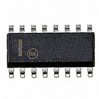
MC14512BDG ON Semiconductor, MC14512BDG Datasheet - Page 5

MC14512BDG
Manufacturer Part Number
MC14512BDG
Description
IC MUX DATA SELECT 8CH 16-SOIC
Manufacturer
ON Semiconductor
Series
4000Br
Type
Data Selector/Multiplexerr
Datasheet
1.MC14512BCPG.pdf
(7 pages)
Specifications of MC14512BDG
Circuit
1 x 8:1
Independent Circuits
1
Voltage Supply Source
Dual Supply
Voltage - Supply
3 V ~ 18 V
Operating Temperature
-55°C ~ 125°C
Mounting Type
Surface Mount
Package / Case
16-SOIC (3.9mm Width)
Logical Function
Mux
Configuration
1 x 8:1
Number Of Inputs
8
Number Of Outputs
1
Operating Supply Voltage (typ)
3.3/5/9/12/15V
Operating Supply Voltage (min)
3V
Operating Supply Voltage (max)
18V
Power Dissipation
500mW
Operating Temp Range
-55C to 125C
Operating Temperature Classification
Military
Mounting
Surface Mount
Pin Count
16
Package Type
SOIC
Product
Decoders, Encoders, Multiplexers & Demultiplexers
Logic Family
MC145
Number Of Bits
8
Number Of Lines (input / Output)
8.0 / 3.0
Propagation Delay Time
650 ns at 5 V, 250 ns at 10 V, 170 ns at 15 V
Supply Voltage (max)
18 V
Supply Voltage (min)
3 V
Maximum Operating Temperature
+ 125 C
Minimum Operating Temperature
- 55 C
Mounting Style
SMD/SMT
Number Of Input Lines
8.0
Number Of Output Lines
3.0
Rohs Compliant
YES
Logic Type
Data Selector / Multiplexer
No. Of Channels
8
Supply Voltage Range
3V To 18V
Logic Case Style
SOIC
No. Of Pins
16
Operating Temperature Range
-55°C To +125°C
Msl
MSL 1 - Unlimited
Lead Free Status / RoHS Status
Lead free / RoHS Compliant
Current - Output High, Low
-
Lead Free Status / Rohs Status
Compliant
Available stocks
Company
Part Number
Manufacturer
Quantity
Price
Company:
Part Number:
MC14512BDG
Manufacturer:
ON Semiconductor
Quantity:
135
Selectors can be connected to a single date bus as shown.
One MC14512B is selected by the 3−state control, and the
remaining devices are disabled into a high−impedance “off”
state. The number of 8−bit data selectors, N, that may be
connected to a bus line is determined from the output drive
current, I
and the load current, I
X0
X1
X2
X3
X4
X5
X6
X7
C
Output terminals of several MC14512B 8−Bit Data
B
A
13
12
11
1
2
3
4
5
6
7
9
OD
, 3−state or disable output leakage current, I
L
, required to drive the bus line
3−STATE MODE OF OPERATION
IN
TRANSMISSION
1
GATE
http://onsemi.com
2
LOGIC DIAGRAM
OUT
MC14512B
TL
,
IN
5
(including fanout to other device inputs), and can be
calculated by:
N must be calculated for both high and low logic state of the
bus line.
V
1
2
DISABLE
SS
INHIBIT
V
15
10
DD
14
Z
OUT
N =
SELECTED
MC14512B
MC14512B
MC14512B
DEVICE
I
OD
I
TL
– I
L
I
I
I
OD
TL
TL
+ 1
DATA
BUS
I
L
LOAD


