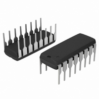
MC74AC138NG ON Semiconductor, MC74AC138NG Datasheet - Page 2

MC74AC138NG
Manufacturer Part Number
MC74AC138NG
Description
IC DECODER/DEMUX 1-8 HS 16DIP
Manufacturer
ON Semiconductor
Series
74ACr
Type
Decoder/Demultiplexerr
Specifications of MC74AC138NG
Circuit
1 x 3:8
Independent Circuits
1
Current - Output High, Low
24mA, 24mA
Voltage Supply Source
Single Supply
Voltage - Supply
2 V ~ 6 V
Operating Temperature
-40°C ~ 85°C
Mounting Type
Through Hole
Package / Case
16-DIP (0.300", 7.62mm)
Product
Decoders, Encoders, Multiplexers & Demultiplexers
Logic Family
74AC
Number Of Lines (input / Output)
1.0 / 8.0
Supply Voltage (max)
6 V
Supply Voltage (min)
2 V
Maximum Operating Temperature
+ 85 C
Minimum Operating Temperature
- 40 C
Mounting Style
Through Hole
Number Of Input Lines
1.0
Number Of Output Lines
8.0
Current, Supply
80 μA
Function Type
1-Channel
Logic Function
Decoder/Demultiplexer
Logic Type
CMOS
Number Of Circuits
Single
Package Type
PDIP-16
Special Features
1-of-8
Temperature, Operating, Range
-40 to +85 °C
Voltage, Supply
5 V
No. Of Outputs
8
Supply Voltage Range
2V To 6V
Logic Case Style
DIP
No. Of Pins
16
Operating Temperature Range
-40°C To +85°C
Filter Terminals
DIP
Rohs Compliant
Yes
Family Type
AC
Lead Free Status / RoHS Status
Lead free / RoHS Compliant
Other names
MC74AC138NGOS
Available stocks
Company
Part Number
Manufacturer
Quantity
Price
Part Number:
MC74AC138NG
Manufacturer:
ON/安森美
Quantity:
20 000
MAXIMUM RATINGS*
V
V
V
I
I
I
T
*Maximum Ratings are those values beyond which damage to the device may occur. Functional operation should be restricted to the Recom-
RECOMMENDED OPERATING CONDITIONS
V
V
t
t
T
T
I
I
1. V
2. V
IN
OUT
CC
r
r
OH
OL
, t
, t
stg
A
mended Operating Conditions.
J
CC
IN
OUT
CC
IN
Symbol
f
f
, V
Symbol
IN
IN
A
A
A
A
A
OUT
0
1
2
3
4
from 30% to 70% V
from 0.8 V to 2.0 V; see individual Data Sheets for devices that differ from the typical input rise and fall times.
0
0
0
0
A
0
0
1
A
0
Supply Voltage
DC Input Voltage, Output Voltage (Ref. to GND)
Input Rise and Fall Time (Note 1)
′AC Devices except Schmitt Inputs
Input Rise and Fall Time (Note 2)
′ACT Devices except Schmitt Inputs
Junction Temperature (PDIP)
Operating Ambient Temperature Range
Output Current − High
Output Current − Low
1
2
A
0
3
2
DC Supply Voltage (Referenced to GND)
DC Input Voltage (Referenced to GND)
DC Output Voltage (Referenced to GND)
DC Input Current, per Pin
DC Output Sink/Source Current, per Pin
DC V
Storage Temperature
0
4
0
5
CC
CC
0
123
6
E
or GND Current per Output Pin
; see individual Data Sheets for devices that differ from the typical input rise and fall times.
H
0
7
0
0
A
0
Figure 4. Expansion to 1−of−32 Decoding
Parameter
1
0
A
0
1
2
A
0
2
3
Parameter
0
4
0
5
0
123
6
E
0
7
3
V
V
V
V
V
CC
CC
CC
CC
CC
0
0
′ACT
′AC
@ 3.0 V
@ 4.5 V
@ 5.5 V
@ 4.5 V
@ 5.5 V
A
0
0
1
A
0
1
2
A
0
2
3
0
4
0
5
Min
−40
2.0
4.5
0
−
−
−
−
−
−
−
−
0
6
123
E
0
7
Typ
150
−0.5 to V
−0.5 to V
5.0
5.0
8.0
40
25
10
25
−
−
−
−
0
0
−0.5 to +7.0
−65 to +150
A
0
Value
0
1
±20
±50
±50
A
0
2
1
CC
CC
0
A
3
+0.5
+0.5
2
Max
V
140
−24
6.0
5.5
85
24
0
CC
−
−
−
−
−
′04
4
0
5
0
123
6
E
0
0
31
7
Unit
Unit
ns/V
ns/V
mA
mA
mA
mA
mA
°C
°C
°C
V
V
V
V
V


