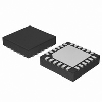
NB7VQ1006MMNTXG ON Semiconductor, NB7VQ1006MMNTXG Datasheet - Page 3

NB7VQ1006MMNTXG
Manufacturer Part Number
NB7VQ1006MMNTXG
Description
IC EQUALIZER RECEIVER 24-QFN
Manufacturer
ON Semiconductor
Datasheet
1.NB7VQ1006MMNTXG.pdf
(10 pages)
Specifications of NB7VQ1006MMNTXG
Logic Type
Equalizer Receiver
Supply Voltage
1.71 V ~ 2.625 V
Number Of Bits
1
Operating Temperature
-40°C ~ 85°C
Mounting Type
Surface Mount
Package / Case
24-TFQFN Exposed Pad
Operating Supply Voltage (min)
1.71V
Operating Supply Voltage (max)
2.625V
Operating Temp Range
-40C to 85C
Operating Temperature Classification
Industrial
Mounting
Surface Mount
Pin Count
24
Supply Voltage (max)
2.625 V
Supply Voltage (min)
1.71 V
Maximum Operating Temperature
+ 85 C
Mounting Style
SMD/SMT
Data Rate
10 Gbps
Minimum Operating Temperature
- 40 C
Supply Current
100 mA, 180 mA
Lead Free Status / RoHS Status
Lead free / RoHS Compliant
Available stocks
Company
Part Number
Manufacturer
Quantity
Price
Part Number:
NB7VQ1006MMNTXG
Manufacturer:
ON/安森美
Quantity:
20 000
1. In the differential configuration when the input termination pin (VT) is connected to a common termination voltage or left open, and if no signal
2. All VCC, VCCO and GND pins must be externally connected to the same power supply voltage to guarantee proper device operation.
Table 2. PIN DESCRIPTION
Pin
10
12
13
14
15
16
17
18
19
20
21
22
23
24
11
1
2
3
4
5
6
7
8
9
−
is applied on IN/IN, then the device will be susceptible to self−oscillation.
EQEN
VCCO
VCCO
Name
GND
GND
GND
GND
VCC
VCC
Q5
Q5
Q4
Q4
Q3
Q3
Q2
Q2
Q1
Q1
Q0
Q0
EP
VT
IN
IN
LVPECL, CML,
LVPECL, CML,
LVCMOS Input
LVDS Input
LVDS Input
CML
CML
CML
CML
CML
CML
CML
CML
CML
CML
CML
CML
I/O
−
Internal 50 W Termination Pin for IN and IN
Negative Supply Voltage
Positive Supply Voltage for the Core Logic
Non−inverted Differential Clock/Data Input. (Note 1)
Inverted Differential Clock/Data Input. (Note 1)
Equalizer Enable Input; pin will default LOW when left open (has internal pull−down resistor)
Positive Supply Voltage for the Core Logic
Inverted Differential Output. Typically terminated with 50 W resistor to V
Non−inverted Differential Output. Typically terminated with 50 W resistor to V
Inverted Differential Output. Typically terminated with 50 W resistor to V
Non−inverted Differential Output. Typically terminated with 50 W resistor to V
Negative Supply Voltage
Positive Supply Voltage for the pre−amplifier and output buffer
Inverted Differential Output. Typically terminated with 50 W resistor to V
Non−inverted Differential Output. Typically terminated with 50 W resistor to V
Inverted Differential Output. Typically terminated with 50 W resistor to V
Non−inverted Differential Output. Typically terminated with 50 W resistor to V
Positive Supply Voltage for the pre−amplifier and output buffer
Negative Supply Voltage
Inverted Differential Output. Typically terminated with 50 W resistor to V
Non−inverted Differential Output. Typically terminated with 50 W resistor to V
Inverted Differential Output. Typically terminated with 50 W resistor to V
Non−inverted Differential Output. Typically terminated with 50 W resistor to V
Negative Supply Voltage
The Exposed Pad (EP) on the QFN−24 package bottom is thermally connected to the die for im-
proved heat transfer out of package. The exposed pad must be attached to a heat−sinking con-
duit. The pad is electrically connected to GND and is recommended to be electrically connected
to GND on the PC board.
http://onsemi.com
3
Description
CC
CC
CC
CC
CC
CC
.
.
.
.
.
.
CC
CC
CC
CC
CC
CC
.
.
.
.
.
.


