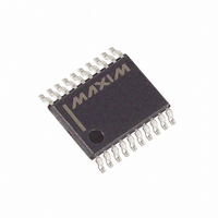
MAX3001EAUP+ Maxim Integrated Products, MAX3001EAUP+ Datasheet - Page 11

MAX3001EAUP+
Manufacturer Part Number
MAX3001EAUP+
Description
IC TRANSLATOR LEVEL 8CH 20-TSSOP
Manufacturer
Maxim Integrated Products
Datasheet
1.MAX3001EEUPT.pdf
(25 pages)
Specifications of MAX3001EAUP+
Logic Function
Translator, Bidirectional, Unidirectional, 3-State
Number Of Bits
8
Input Type
CMOS
Output Type
CMOS
Data Rate
35Mbps
Number Of Channels
8
Number Of Outputs/channel
1
Differential - Input:output
No/No
Propagation Delay (max)
8.5ns
Voltage - Supply
1.65 V ~ 5.5 V
Operating Temperature
-40°C ~ 125°C
Package / Case
20-TSSOP
Supply Voltage
1.2 V ~ 5.5 V
Lead Free Status / RoHS Status
Lead free / RoHS Compliant
MAX3003
TSSOP
10
11
12
13
14
15
16
17
18
19
20
—
1
2
3
4
5
6
7
8
9
+1.2V to +5.5V, ±15kV ESD-Protected, 0.1µA,
UCSP
PIN
C5
D5
C4
D4
C3
D3
C2
D2
D1
C1
B1
A1
A2
B2
A3
B3
A4
B4
A5
B5
—
______________________________________________________________________________________
TQFN
19
20
10
11
12
13
14
15
16
17
18
EP
1
2
3
4
5
6
7
8
9
35Mbps, 8-Channel Level Translators
I/O V
I/O V
I/O V
I/O V
I/O V
I/O V
I/O V
I/O V
I/O V
I/O V
I/O V
I/O V
I/O V
I/O V
I/O V
I/O V
EN A/B
NAME
GND
V
EP
V
CC
CC
CC
CC
CC
CC
CC
CC
CC
L
L
L
L
L
L
L
L
L
1A
2A
3A
4A
1B
2B
3B
4B
4B
3B
2B
1B
4A
3A
2A
1A
Input/Output 1A, Referenced to V
Logic Input Voltage, +1.2V ≤ V
Input/Output 2A, Referenced to V
Input/Output 3A, Referenced to V
Input/Output 4A, Referenced to V
Input/Output 1B, Referenced to V
Input/Output 2B, Referenced to V
Input/Output 3B, Referenced to V
Input/Output 4B, Referenced to V
Enable Input. If EN A/B is pulled low, channels 1B through 4B are active, and channels
1A through 4A are in three-state. If EN A/B is driven high to V
are active, and channels 1B through 4B are in three-state.
Ground
Input/Output 4B, Referenced to V
Input/Output 3B, Referenced to V
Input/Output 2B, Referenced to V
Input/Output 1B, Referenced to V
Input/Output 4A, Referenced to V
Input/Output 3A, Referenced to V
Input/Output 2A, Referenced to V
V
Input/Output 1A, Referenced to V
Exposed Pad. Connect to GND.
CC
Input Voltage, +1.65V ≤ V
CC
L
≤ V
L
L
L
L
L
L
L
L
CC
CC
CC
CC
CC
CC
CC
CC
≤ +5.5V. Bypass V
CC
Pin Description (continued)
FUNCTION
. Bypass V
L
to GND with a 0.1µF capacitor.
CC
to GND with a 0.1µF capacitor.
L
, channels 1A through 4A
11


