NLSX3373MUTAG ON Semiconductor, NLSX3373MUTAG Datasheet
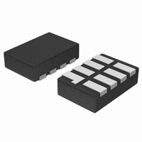
IC XLATOR 2BIT 20MBPS 8-UDFN

NLSX3373MUTAG

Manufacturer Part Number
NLSX3373MUTAG
Description
IC XLATOR 2BIT 20MBPS 8-UDFN
Manufacturer
ON Semiconductor
Datasheet

Specifications of NLSX3373MUTAG

Logic Function
Translator, Bidirectional, Open Drain
Number Of Bits
2
Input Type
Voltage
Output Type
Voltage
Data Rate
8Mbps
Number Of Channels
2
Number Of Outputs/channel
1
Differential - Input:output
No/No
Propagation Delay (max)
30ns
Voltage - Supply
1.65 V ~ 5.5 V
Operating Temperature
-40°C ~ 85°C
Package / Case
8-UFDFN
Supply Voltage
1.65 V ~ 5.5 V
Lead Free Status / RoHS Status
Lead free / RoHS Compliant

Available stocks

Company
Part Number
Manufacturer
Quantity
Price
Part Number:
NLSX3373MUTAG
Manufacturer:
ONSEMI
Quantity:
42 480
NLSX3373
2-Bit 20 Mb/s Dual-Supply
Level Translator
auto sensing translator that does not require a directional control pin.
The V
power supply rails, V
configurable from 1.65 V to 4.5 V while V
configurable to 1.2 V to 4.1 V. This allows lower voltage logic
signals on the V
signals on the V
10 kW pullup resistors on the I/O lines. The integrated pullup
resistors are used to pullup the I/O lines to either V
NLSX3373 is an excellent match for open−drain applications such as
the I
Features
Typical Applications
Important Information
© Semiconductor Components Industries, LLC, 2008
July, 2008 − Rev. 5
The NLSX3373 is a 2−bit configurable dual−supply bidirectional
The NLSX3373 translator has open−drain outputs with integrated
Wide Low−Side V
4.5 V
Wide High−Side V
High−Speed with 20 Mb/s Guaranteed Date Rate for V
Low Bit−to−Bit Skew
Enable Input and I/O Lines have Overvoltage Tolerant (OVT) to
Nonpreferential Powerup Sequencing
Integrated 10 kW Pullup Resistors
Small Space Saving Package − 1.8 x 1.2 x 0.5 mm UDFN8
This is a Pb−Free Device
I
Low Voltage ASIC Level Translation
Mobile Phones, PDAs, Cameras
ESD Protection for Power, Enable and I/O Pins:
2
C, SMBus, PMBus
2
C communication bus.
CC
I/O and V
Human Body Model (HBM): $7.5 kV
Machine Model (MM): 400 V
CC
L
side, and vice−versa.
side to be translated into higher voltage logic
L
L
CC
CC
I/O ports are designed to track two different
Operating Range: 1.2 V to 4.1 V
and V
Operating Range: 1.65 V to 4.5 V
L
respectively. The V
L
CC
supply rail is
L
supply rail is
or V
L
> 2.5 V
1
CC
. The
I/O V
I/O V
†For information on tape and reel specifications,
NLSX3373MUTAG
including part orientation and tape sizes, please
refer to our Tape and Reel Packaging Specification
Brochure, BRD8011/D.
EN
L
L
1
1
2
Device
I/O V
I/O V
ORDERING INFORMATION
8
VB = Specific Device Code
M
G
GND
V
L
L
http://onsemi.com
PIN ASSIGNMENT
LOGIC DIAGRAM
1
2
L
CASE 517AJ
= Date Code
= Pb−Free Package
MU SUFFIX
1
2
3
4
UDFN8
(Top View)
(Pb−Free)
Package
UDFN8
Publication Order Number:
8
7
6
5
3000/T ape & Reel
V
V
I/O V
I/O V
EN
MARKING
DIAGRAM
L
CC
Shipping
NLSX3373/D
V
VBM
CC
CC
CC
G
I/O V
I/O V
1
2
GND
CC
CC
1
2

Related parts for NLSX3373MUTAG

NLSX3373MUTAG Summary of contents

Page 1

... I I I/O V I/O V GND ORDERING INFORMATION Device NLSX3373MUTAG †For information on tape and reel specifications, including part orientation and tape sizes, please refer to our Tape and Reel Packaging Specification Brochure, BRD8011/D. 1 http://onsemi.com MARKING DIAGRAM UDFN8 VBM MU SUFFIX G CASE 517AJ = Date Code = Pb− ...

Page 2

V L PU1 R Pullup PIN ASSIGNMENT Pins Description V V Input Voltage Input Voltage L L GND Ground EN Output Enable I I/O Port, Referenced to V ...

Page 3

MAXIMUM RATINGS Symbol Parameter V High−side DC Supply Voltage CC V High−side DC Supply Voltage L I −Referenced DC Input/Output Voltage −Referenced DC Input/Output Voltage Enable Control Pin DC Input ...

Page 4

DC ELECTRICAL CHARACTERISTICS Symbol Parameter V I/O V Input HIGH Voltage IHC CC V I/O V Input LOW Voltage ILC CC V I/O V Input HIGH Voltage IHL L V I/O V Input LOW Voltage ILL L V Control Pin ...

Page 5

TIMING CHARACTERISTICS − RAIL−TO−RAIL DRIVING CONFIGURATIONS (I/O test circuit of Figures 2 and 3, C LOAD Symbol Parameter +1 +4 I/O V Risetime RVCC CC t I/O V Falltime FVCC CC ...

Page 6

TIMING CHARACTERISTICS − OPEN DRAIN DRIVING CONFIGURATIONS (I/O test circuit of Figures 4 and 5, C LOAD Symbol Parameter +1 +4 I/O V Risetime RVCC CC t I/O V Falltime FVCC ...

Page 7

NLSX3373 I Source Figure 2. Rail−to−Rail Driving I/O V NLSX3373 I Figure 4. Open−Drain Driving I I/O V RISE/FALL 90% 50% 10% t PD_VL−VCC ...

Page 8

PULSE GENERATOR PZH PHZ PZL PLZ equivalent (Includes jig and probe capacitance OUT Figure 7. Test Circuit for Enable/Disable ...

Page 9

Level Translator Architecture The NLSX3373 auto sense translator provides bi−directional voltage level shifting to transfer data in multiple supply voltage systems. This device has two supply voltages, V and V , which set the logic levels the ...

Page 10

... SCILLC is an Equal Opportunity/Affirmative Action Employer. This literature is subject to all applicable copyright laws and is not for resale in any manner. PUBLICATION ORDERING INFORMATION LITERATURE FULFILLMENT: Literature Distribution Center for ON Semiconductor P.O. Box 5163, Denver, Colorado 80217 USA Phone: 303−675−2175 or 800−344−3860 Toll Free USA/Canada Fax: 303− ...

Related keywords