MC100EP91MNR2G ON Semiconductor, MC100EP91MNR2G Datasheet - Page 4
MC100EP91MNR2G
Manufacturer Part Number
MC100EP91MNR2G
Description
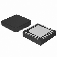
TRANSLATOR NECL OUTPUT 24-QFN
Manufacturer
ON Semiconductor
Series
100EPr
Datasheet
1.MC100EP91MNR2G.pdf
(10 pages)
Specifications of MC100EP91MNR2G
Logic Function
Translator
Number Of Bits
3
Input Type
AnyLevel™
Output Type
NECL
Number Of Channels
3
Number Of Outputs/channel
1
Differential - Input:output
Yes/Yes
Propagation Delay (max)
0.675ns
Voltage - Supply
2.375 V ~ 3.8 V
Operating Temperature
-40°C ~ 85°C
Package / Case
24-TFQFN Exposed Pad
Supply Voltage
2.375 V ~ 3.8 V
Lead Free Status / RoHS Status
Lead free / RoHS Compliant
Data Rate
-
Lead Free Status / Rohs Status
Compliant
Other names
MC100EP91MNR2G
MC100EP91MNR2GOSTR
MC100EP91MNR2GOSTR
Available stocks
Company
Part Number
Manufacturer
Quantity
Price
Company:

Part Number:
MC100EP91MNR2G
Manufacturer:
ON Semiconductor
Quantity:
440


Stresses exceeding Maximum Ratings may damage the device. Maximum Ratings are stress ratings only. Functional operation above the
Recommended Operating Conditions is not implied. Extended exposure to stresses above the Recommended Operating Conditions may affect
device reliability.
NOTE: Device will meet the specifications after thermal equilibrium has been established when mounted in a test socket or printed circuit
3. Input parameters vary 1:1 with V
4. V
Table 3. MAXIMUM RATINGS
Symbol
Table 4. DC CHARACTERISTICS POSITIVE INPUTS
Symbol
V
V
V
V
I
I
T
T
q
q
q
T
I
V
V
V
I
I
out
BB
CC
IH
IL
A
stg
JA
JA
JC
sol
CC
EE
I
OP
IH
IL
IHCMR
IHCMR
board with maintained transverse airflow greater than 500 lfpm. Electrical parameters are guaranteed only over the declared
operating temperature range. Functional operation of the device exceeding these conditions is not implied. Device specification limit
values are applied individually under normal operating conditions and not valid simultaneously.
min varies 1:1 with GND. V
Positive Power Supply
Negative Power Supply
Positive Input Voltage
Operating Voltage
Output Current
PECL V
Operating Temperature Range
Storage Temperature Range
Thermal Resistance (Junction−to−Ambient)
JESD 51−3 (1S−Single Layer Test Board)
Thermal Resistance (Junction−to−Ambient)
JESD 51−6 (2S2P Multilayer Test Board) with Filled Thermal Vias
Thermal Resistance (Junction−to−Case)
Wave Solder
Positive Power Supply Current
Input HIGH Voltage (Single−Ended)
Input LOW Voltage (Single−Ended)
Input HIGH Voltage Common Mode Range
(Differential Configuration) (Note 4)
Input HIGH Current (@ V
Input LOW Current (@ V
BB
Sink/Source
Characteristic
CC
IL
IH
Parameter
)
. V
IHCMR
)
CC
can vary +1.3 V / −0.125 V.
max varies 1:1 with V
http://onsemi.com
D
D
V
CC
1335
GND
−150
Min
0.5
10
0
CC
Pb−Free
= 2.5 V, V
4
.
−40°C
Typ
Pb
14
EE
GND = 0 V
GND = 0 V
GND = 0 V
GND = 0 V
Continuous
Surge
0 lfpm
500 lfpm
0 lfpm
500 lfpm
Standard Board
Max
V
875
150
= −3.0 V to −5.5 V, GND = 0 V (Note 3)
2.5
20
CC
Condition 1
1335
GND
−150
Min
0.5
10
0
25°C
Typ
14
Condition 2
V
Max
V
V
SOIC−20
SOIC−20
SOIC−20
875
150
2.5
QFN−24
QFN−24
QFN−24
20
CC
I
CC
V
− V
CC
EE
1335
GND
−150
Min
0.5
10
0
−65 to +150
85°C
−40 to +85
30 to 35
3.8 to 0
3.8 to 0
Typ
Rating
14
± 0.5
100
225
225
9.8
−6
50
90
60
37
32
11
Max
V
875
150
2.5
20
CC
°C/W
°C/W
°C/W
°C/W
°C/W
°C/W
Unit
Unit
mA
mA
mA
mA
mV
mV
°C
°C
°C
mA
mA
V
V
V
V
V
Related parts for MC100EP91MNR2G
Image
Part Number
Description
Manufacturer
Datasheet
Request
R

Part Number:
Description:
NECL Output Translator
Manufacturer:
ON Semiconductor
Datasheet:
Part Number:
Description:
ON Semiconductor [VOLTAGE REGULATOR]
Manufacturer:
ON Semiconductor
Datasheet:
Part Number:
Description:
357-036-542-201 CARDEDGE 36POS DL .156 BLK LOPRO
Manufacturer:
ON Semiconductor
Datasheet:
Part Number:
Description:
357-036-542-201 CARDEDGE 36POS DL .156 BLK LOPRO
Manufacturer:
ON Semiconductor
Datasheet:
Part Number:
Description:
357-036-542-201 CARDEDGE 36POS DL .156 BLK LOPRO
Manufacturer:
ON Semiconductor
Datasheet:
Part Number:
Description:
357-036-542-201 CARDEDGE 36POS DL .156 BLK LOPRO
Manufacturer:
ON Semiconductor
Datasheet:
Part Number:
Description:
357-036-542-201 CARDEDGE 36POS DL .156 BLK LOPRO
Manufacturer:
ON Semiconductor
Datasheet:
Part Number:
Description:
357-036-542-201 CARDEDGE 36POS DL .156 BLK LOPRO
Manufacturer:
ON Semiconductor
Datasheet:
Part Number:
Description:
357-036-542-201 CARDEDGE 36POS DL .156 BLK LOPRO
Manufacturer:
ON Semiconductor
Datasheet:
Part Number:
Description:
357-036-542-201 CARDEDGE 36POS DL .156 BLK LOPRO
Manufacturer:
ON Semiconductor
Datasheet:
Part Number:
Description:
357-036-542-201 CARDEDGE 36POS DL .156 BLK LOPRO
Manufacturer:
ON Semiconductor
Datasheet:
Part Number:
Description:
357-036-542-201 CARDEDGE 36POS DL .156 BLK LOPRO
Manufacturer:
ON Semiconductor
Datasheet:
Part Number:
Description:
Manufacturer:
ON Semiconductor
Datasheet:
Part Number:
Description:
Manufacturer:
ON Semiconductor
Datasheet: