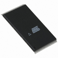
AT49F008AT-12TC Atmel, AT49F008AT-12TC Datasheet - Page 5

AT49F008AT-12TC
Manufacturer Part Number
AT49F008AT-12TC
Description
IC FLASH 8MBIT 120NS 48TSOP
Manufacturer
Atmel
Datasheet
1.AT49F008AT-12TC.pdf
(18 pages)
Specifications of AT49F008AT-12TC
Format - Memory
FLASH
Memory Type
FLASH
Memory Size
8M (1M x 8 or 512K x 16)
Speed
120ns
Interface
Parallel
Voltage - Supply
4.5 V ~ 5.5 V
Operating Temperature
0°C ~ 70°C
Package / Case
48-TSOP
Lead Free Status / RoHS Status
Contains lead / RoHS non-compliant
Available stocks
Company
Part Number
Manufacturer
Quantity
Price
Company:
Part Number:
AT49F008AT-12TC
Manufacturer:
PHILIPS
Quantity:
6
AT49F008A(T)/8192A(T)
Once the feature is enabled, the data in the boot block can no longer be erased or pro-
grammed when input levels of 5.5V or less are used. Data in the main memory block can still
be changed through the regular programming method. To activate the lockout feature, a series
of six program commands to specific addresses with specific data must be performed. Please
refer to the Command Definitions table.
BOOT BLOCK LOCKOUT DETECTION: A software method is available to determine if pro-
gramming of the boot block section is locked out. When the device is in the software product
identification mode (see Software Product Identification Entry and Exit sections), a read from
the following address location will show if programming the boot block is locked out – 00002H
for the AT49F008A and AT49F8192A; FC002H for the AT49F008AT; and 7E002H for the
AT49F8192AT. If the data on I/O0 is low, the boot block can be programmed; if the data on
I/O0 is high, the program lockout feature has been enabled and the block cannot be pro-
grammed. The software product identification exit code should be used to return to standard
operation.
BOOT BLOCK PROGRAMMING LOCKOUT OVERRIDE: The user can override the boot
block programming lockout by taking the RESET pin to 12 volts during the entire chip erase,
sector erase or word programming operation. When the RESET pin is brought back to TTL
levels, the boot block programming lockout feature is again active.
PRODUCT IDENTIFICATION: The product identification mode identifies the device and man-
ufacturer as Atmel. It may be accessed by hardware or software operation. The hardware
operation mode can be used by an external programmer to identify the correct programming
algorithm for the Atmel product.
For details, see “Operating Modes” (for hardware operation) or “Software Product Identifica-
tion Entry/Exit” on page 13. The manufacturer and device codes are the same for both modes.
DATA POLLING: The AT49F008A(T)/8192A(T) features Data Polling to indicate the end of a
program cycle. During a program cycle an attempted read of the last byte loaded will result in
the complement of the loaded data on I/O7. Once the program cycle has been completed, true
data is valid on all outputs and the next cycle may begin. During a chip or sector erase opera-
tion, an attempt to read the device will give a “0” on I/O7. Once the program or erase cycle has
completed, true data will be read from the device. Data Polling may begin at any time during
the program cycle.
TOGGLE BIT: In addition to Data Polling, the AT49F008A(T)/8192A(T) provides another
method for determining the end of a program or erase cycle. During a program or erase oper-
ation, successive attempts to read data from the device will result in I/O6 toggling between
one and zero. Once the program cycle has completed, I/O6 will stop toggling and valid data
will be read. Examining the toggle bit may begin at any time during a program cycle.
READY/BUSY: For the AT49F008A(T), pin 12 is an open-drain Ready/Busy output pin, which
provides another method of detecting the end of a program or erase operation. RDY/BUSY is
actively pulled low during the internal program and erase cycles and it is released at the com-
pletion of the cycle. The open-drain connection allows for OR-tying of several devices to the
same RDY/BUSY line.
HARDWARE DATA PROTECTION: Hardware features protect against inadvertent programs
to the AT49F008A(T)/8192A(T) in the following ways: (a) V
sense: if V
is below 3.8V (typ-
CC
CC
ical), the program function is inhibited. (b) V
power-on delay: once V
has reached the V
CC
CC
CC
sense level, the device will automatically time-out 10 ms (typical) before programming. (c) Pro-
gram inhibit: holding any one of OE low, CE high or WE high inhibits program cycles. (d) Noise
filter: pulses of less than 15 ns (typical) on the WE or CE inputs will not initiate a program
cycle.
5
1199G–FLASH–11/02


