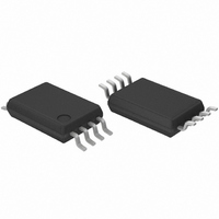
BR93L46RFV-WE2 Rohm Semiconductor, BR93L46RFV-WE2 Datasheet - Page 13

BR93L46RFV-WE2
Manufacturer Part Number
BR93L46RFV-WE2
Description
IC EEPROM 1KBIT 2MHZ 8SSOP
Manufacturer
Rohm Semiconductor
Datasheet
1.BR93L56RFVM-WTR.pdf
(41 pages)
Specifications of BR93L46RFV-WE2
Format - Memory
EEPROMs - Serial
Memory Type
EEPROM
Memory Size
1K (64 x 16)
Speed
2MHz
Interface
Microwire, 3-Wire Serial
Voltage - Supply
1.8 V ~ 5.5 V
Operating Temperature
-40°C ~ 85°C
Package / Case
8-SSOP
Lead Free Status / RoHS Status
Lead free / RoHS Compliant
Other names
BR93L46RFV-WE2
BR93L46RFV-WE2TR
BR93L46RFV-WE2TR
Available stocks
Company
Part Number
Manufacturer
Quantity
Price
Part Number:
BR93L46RFV-WE2
Manufacturer:
ROHM/罗姆
Quantity:
20 000
© 2011 ROHM Co., Ltd. All rights reserved.
BR93L□□-W Series, 93A□□-WM Series, BR93H□□-WC Series
www.rohm.com
4) Write enable (WEN) / disable (WDS) cycle
○ At power on, this IC is in write disable status by the internal RESET circuit. Before executing the write command, it is
○ When the write enable command is executed after power on, write enable status gets in. When the write disable command
5) Erase cycle timing (ERASE)
○In this command, data of the designated address is made into “1”. The data of the designated address becomes “FFFFh”.
6) Chip erase cycle timing (ERAL)
○In this command, data of all addresses is erased. Data of all addresses becomes ”FFFFh”.
Actual ERASE starts at the fall of CS after the fall of A0 taken SK clock.
In ERASE, status can be detected in the same manner as in WRITE command.
Actual ERASE starts at the fall of CS after the falll of the n-th clock from the start bit input.
In ERAL, status can be detected in the same manner as in WRITE command.
necessary to execute the write enable command. And, once this command is executed, it is valid unitl the write disable
command is executed or the power is turned off. However, the read command is valid irrespective of write enable / diable
command. Input to SK after 6 clocks of this command is available by either “H” or “L”, but be sure to input it.
is executed then, the IC gets in write disable status as same as at power on, and then the write command is canceled
thereafter in software manner. However, the read command is executable. In write enable status, even when the write
command is input by mistake, write is started. To prevent such a mistake, it is recommended to execute the write disable
command after completion of write.
CS
SK
DI
DO
CS
SK
DI
DO
CS
SK
DI
DO
High-Z
High-Z
High-Z
1
1
1
1
Fig.63 Write enable (WEN) / disable (WDS) cycle
Fig.64 Erase cycle timing
Fig.65 Chip erase cycle timing
1
1
1
2
0
2
1
0
0
2
Am
0
1
3
4
4
4
0
~ ~
~ ~
~ ~
~ ~
~ ~
A3
5
DISABLE=0 0
ENABLE=1 1
A2
6
A1
7
~ ~
A0
~ ~
8
tCS
n
13/40
tCS
n
~ ~
~ ~
~ ~
~ ~
n
tE/W
tE/W
BUSY
tSV
BUSY
~ ~
~ ~
~ ~
~ ~
~ ~
STATUS
~ ~
~ ~
~ ~
tSV
~ ~
~ ~
STATUS
READY
READY
~ ~
~ ~
~ ~
~ ~
~ ~
~ ~
~ ~
~ ~
~ ~
~ ~
BR93L46-W/A46-WM : n=9
BR93L56-W/A56-WM
BR93L66-W/A66-WM
BR93L76-W/A76-WM
BR93L86-W/A86-WM
BR93L46-W/A46-WM : n=9, m=5
BR93L56-W/A56-WM
BR93L66-W/A66-WM
BR93L76-W/A76-WM
BR93L86-W/A86-WM
BR93L46-W/A46-WM : n=9
BR93L56-W/A56-WM
BR93L66-W/A66-WM
BR93L76-W/A76-WM
BR93L86-W/A86-WM
: n=11
: n=13
Technical Note
2011.02 - Rev.F
: n=11, m=7
: n=13, m=9
: n=11
: n=13


