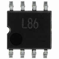
BR93L86F-WE2 Rohm Semiconductor, BR93L86F-WE2 Datasheet - Page 15

BR93L86F-WE2
Manufacturer Part Number
BR93L86F-WE2
Description
IC EEPROM 16KBIT 2MHZ 8SOP
Manufacturer
Rohm Semiconductor
Datasheet
1.BR93L56RFVM-WTR.pdf
(41 pages)
Specifications of BR93L86F-WE2
Format - Memory
EEPROMs - Serial
Memory Type
EEPROM
Memory Size
16K (1K x 16)
Speed
2MHz
Interface
Microwire, 3-Wire Serial
Voltage - Supply
1.8 V ~ 5.5 V
Operating Temperature
-40°C ~ 85°C
Package / Case
8-SOP
Lead Free Status / RoHS Status
Lead free / RoHS Compliant
Other names
BR93L86F-WE2TR
Available stocks
Company
Part Number
Manufacturer
Quantity
Price
Part Number:
BR93L86F-WE2
Manufacturer:
ROHM/罗姆
Quantity:
20 000
© 2011 ROHM Co., Ltd. All rights reserved.
BR93L□□-W Series, 93A□□-WM Series, BR93H□□-WC Series
www.rohm.com
2) At standby
○ERASE, ERAL
○Standby current
○Timing
a:From start bit to 9 clock rise
b:9 clock rise and after
a:From start bit to 13 clock rise
b:13 clock rise and after
c:14 clock rise and after
When CS is “L”, SK input is “L”, DI input is “H”, and even with middle electric potential, current does not increase.
As shown in Fig.69, when SK at standby is “H”, if CS is started, DI status may be read at the rise edge.
At standby and at power ON/OFF, when to start CS, set SK input or DI input to “L” status. (Refer to Fig.70)
designated address data is not guaranteed, therefore write once again.
However, when write is started in b area (CS is ended), cancellation is not
available by any means.
And when SK clock is output continuously is not available.
Cancel by CS=“L”
Cancellation is not available by any means. If Vcc is made OFF in this area,
designated address data is not guaranteed, therefore write once again.
And when SK clock is input continuously, cancellation is not available.
Cancel by CS=“L”
Cancellation is not available by any means. If Vcc is made OFF in this area,
Cancel by CS=“L”
Start bit
Start bit
1bit
1bit
Fig.68 ERASE, ERAL cancel available timing
CS
SK
DI
Fig.69 Wrong action timing
CS=SK=DI=”H”
Wrong recognition as a start bit
Ope code
*
Ope code
2
2bit
a
2bit
Start bit input
*
2
a
Address
Address
10bit
6bit
*1
b
*1
tE/W
tE/W
c
1/2
b
15/40
SK
DI
9 Rise of clock
SK
DI
13 Rise of clock
A1
Enlarged figure
CS
SK
DI
D1
a
8
Enlarged figure
12
*1 Address is 8 bits in BR93L56-W/A56-WM, BR93L66-W/A66-WM
*2 11 clocks in BR93L56-W/A56-WM, BR93L66-W/A66-WM
A0
9
Fig.70 Normal action timing
*
13
Note 1) If Vcc is made OFF in this area, designated address data is
Note 2) If CS is started at the same timing as that of the SK rise,
2
b
Address is 10 bits in BR93L76-W/A76-WM
13 clocks in BR93L76-W/A76-WM
If CS is started when SK=”L” or DI=”L”, a start
bit is recognized correctly.
(In the case of BR93L46-W/A46-WM)
(In the case of BR93L86-W/A86-WM)
*2
14
not guaranteed, therefore write once again.
write execution/cancel becomes unstable, therefore, it is
recommended to fail in SK=”L” area.
As for SK rise, recommend timing of tCSS/tCSH or higher.
c
15
Start bit input
Technical Note
2011.02 - Rev.F


