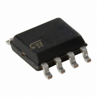
M24512-WMN6TP STMicroelectronics, M24512-WMN6TP Datasheet - Page 14

M24512-WMN6TP
Manufacturer Part Number
M24512-WMN6TP
Description
IC EEPROM 512KBIT 400KHZ 8SOIC
Manufacturer
STMicroelectronics
Specifications of M24512-WMN6TP
Format - Memory
EEPROMs - Serial
Memory Type
EEPROM
Memory Size
512K (64K x 8)
Speed
400kHz
Interface
I²C, 2-Wire Serial
Voltage - Supply
2.5 V ~ 5.5 V
Operating Temperature
-40°C ~ 85°C
Package / Case
8-SOIC (3.9mm Width)
Density
512Kb
Interface Type
Serial (I2C)
Organization
64Kx8
Access Time (max)
900ns
Frequency (max)
400KHz
Write Protection
Yes
Data Retention
40Year
Operating Supply Voltage (typ)
3.3/5V
Operating Temp Range
-40C to 85C
Supply Current
5mA
Operating Supply Voltage (min)
2.5V
Operating Supply Voltage (max)
5.5V
Operating Temperature Classification
Industrial
Mounting
Surface Mount
Pin Count
8
Lead Free Status / RoHS Status
Lead free / RoHS Compliant
Other names
497-8626-2
M24512-WMN6TP
M24512-WMN6TP
Available stocks
Company
Part Number
Manufacturer
Quantity
Price
Company:
Part Number:
M24512-WMN6TP
Manufacturer:
ELO
Quantity:
100
Company:
Part Number:
M24512-WMN6TP
Manufacturer:
STMicroelectronics
Quantity:
68 554
Part Number:
M24512-WMN6TP
Manufacturer:
ST
Quantity:
20 000
Device operation
3.5
3.6
14/41
Addressing the memory array
To start communication between the bus master and the slave device, the bus master must
initiate a Start condition. Following this, the bus master sends the device select code, shown
in
The device select code consists of a 4-bit device type identifier, and a 3-bit Chip Enable
“Address” (E2, E1, E0). To address the memory array, the 4-bit Device Type Identifier is
1010b.
Up to eight memory devices can be connected on a single I
unique 3-bit code on the Chip Enable (E0, E1, E2) inputs. When the device select code is
received, the device only responds if the Chip Enable Address is the same as the value on
the Chip Enable (E0, E1, E2) inputs.
The 8
If a match occurs on the device select code, the corresponding device gives an
acknowledgment on Serial Data (SDA) during the 9
the device select code, it deselects itself from the bus, and goes into Standby mode.
Table 6.
1. X = V
Addressing the Identification page (M24512-DR only)
The M24512-DR features an additional memory page, referred to as Identification page.
Read and write operations can be performed on this page, except if a Lock instruction has
been issued to permanently write protect it.
The M24512-DR Identification page is addressed in the same way as the memory array,
except that the 4-bit device type identifier of the device select code is 1011b (see
Current Address
Read
Random Address
Read
Sequential Read
Byte Write
Page Write
Table 2
th
Mode
IH
bit is the Read/Write bit (RW). This bit is set to 1 for Read and 0 for Write operations.
or V
(on Serial Data (SDA), most significant bit first).
Operating modes
IL
.
RW bit
1
0
1
1
0
0
WC
Doc ID 16459 Rev 22
V
V
X
X
X
X
IL
IL
(1)
Bytes
128
1
1
1
1
th
Start, device select, RW = 1
Start, device select, RW = 0, Address
re-Start, device select, RW = 1
Similar to Current or Random Address
Read
Start, device select, RW = 0
Start, device select, RW = 0
bit time. If the device does not match
M24512-R, M24512-W, M24512-DR
2
C bus. Each one is given a
Initial sequence
Table
3).


