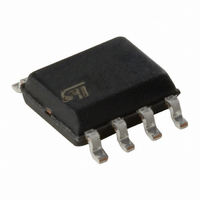
M95M01-RMN6TP STMicroelectronics, M95M01-RMN6TP Datasheet - Page 20

M95M01-RMN6TP
Manufacturer Part Number
M95M01-RMN6TP
Description
IC EEPROM 1MBIT 5MHZ 8SOIC
Manufacturer
STMicroelectronics
Datasheet
1.M95M01-RMN6TP.pdf
(41 pages)
Specifications of M95M01-RMN6TP
Format - Memory
EEPROMs - Serial
Memory Type
EEPROM
Memory Size
1M (128K x 8)
Speed
5MHz
Interface
SPI, 3-Wire Serial
Voltage - Supply
1.8 V ~ 5.5 V
Operating Temperature
-40°C ~ 85°C
Package / Case
8-SOIC (3.9mm Width)
Organization
128 K x 8
Interface Type
SPI
Maximum Clock Frequency
5 MHz
Access Time
80 ns
Supply Voltage (max)
5.5 V
Supply Voltage (min)
1.8 V
Maximum Operating Current
5 mA
Maximum Operating Temperature
+ 85 C
Mounting Style
SMD/SMT
Minimum Operating Temperature
- 40 C
Operating Supply Voltage
2.5 V, 3.3 V, 5 V
Lead Free Status / RoHS Status
Lead free / RoHS Compliant
Other names
497-8701-2
M95M01-RMN6TP
M95M01-RMN6TP
Available stocks
Company
Part Number
Manufacturer
Quantity
Price
Company:
Part Number:
M95M01-RMN6TP
Manufacturer:
INFINEON
Quantity:
23
Company:
Part Number:
M95M01-RMN6TP
Manufacturer:
STMicroelectronics
Quantity:
76 802
Part Number:
M95M01-RMN6TP
Manufacturer:
ST
Quantity:
20 000
Instructions
6.4
20/41
Write Status Register (WRSR)
The Write Status Register (WRSR) instruction allows new values to be written to the Status
Register. Before it can be accepted, a Write Enable (WREN) instruction must previously
have been executed. After the Write Enable (WREN) instruction has been decoded and
executed, the device sets the Write Enable Latch (WEL).
The Write Status Register (WRSR) instruction is entered by driving Chip Select (S) low,
followed by the instruction code and the data byte on Serial Data Input (D).
The instruction sequence is shown in
The Write Status Register (WRSR) instruction has no effect on b6, b5, b4, b1 and b0 of the
Status Register. b6, b5 and b4 are always read as 0.
Chip Select (S) must be driven high after the rising edge of Serial Clock (C) that latches in
the eighth bit of the data byte, and before the next rising edge of Serial Clock (C). Otherwise,
the Write Status Register (WRSR) instruction is not executed. As soon as Chip Select (S) is
driven high, the self-timed Write Status Register cycle (whose duration is t
While the Write Status Register cycle is in progress, the Status Register may still be read to
check the value of the Write In Progress (WIP) bit. The Write In Progress (WIP) bit is 1
during the self-timed Write Status Register cycle, and is 0 when it is completed. When the
cycle is completed, the Write Enable Latch (WEL) is reset.
Figure 11. Write Status Register (WRSR) sequence
S
C
D
Q
0
1
High Impedance
2
Instruction
Doc ID 13264 Rev 7
3
4
5
Figure
6
7
MSB
11.
7
8
6
9 10 11 12 13 14 15
5
Register In
4
Status
3
2
1
0
M95M01-R, M95M01-W
AI02282D
W
) is initiated.


