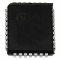
M27C512-70C6 STMicroelectronics, M27C512-70C6 Datasheet - Page 5

M27C512-70C6
Manufacturer Part Number
M27C512-70C6
Description
IC OTP 512KBIT 70NS 32PLCC
Manufacturer
STMicroelectronics
Datasheet
1.M27C512-90B6.pdf
(22 pages)
Specifications of M27C512-70C6
Format - Memory
EPROMs
Memory Type
OTP EPROM
Memory Size
512K (64K x 8)
Speed
70ns
Interface
Parallel
Voltage - Supply
4.5 V ~ 5.5 V
Operating Temperature
-40°C ~ 85°C
Package / Case
32-PLCC
Lead Free Status / RoHS Status
Lead free / RoHS Compliant
Other names
497-1678-5
Available stocks
Company
Part Number
Manufacturer
Quantity
Price
Company:
Part Number:
M27C512-70C6
Manufacturer:
LINFINITY
Quantity:
2 500
Company:
Part Number:
M27C512-70C6
Manufacturer:
STMicroelectronics
Quantity:
10 000
Part Number:
M27C512-70C6
Manufacturer:
ST
Quantity:
20 000
Company:
Part Number:
M27C512-70C6TR
Manufacturer:
STMicroelectronics
Quantity:
10 000
M27C512
2
2.1
2.2
Device operation
The modes of operations of the M27C512 are listed in the Operating Modes table. A single
power supply is required in the read mode. All inputs are TTL levels except for GV
12V on A9 for Electronic Signature.
Read mode
The M27C512 has two control functions, both of which must be logically active in order to
obtain data at the outputs. Chip Enable (E) is the power control and should be used for
device selection. Output Enable (G) is the output control and should be used to gate data to
the output pins, independent of device selection. Assuming that the addresses are stable,
the address access time (t
available at the output after a delay of t
been low and the addresses have been stable for at least t
Standby mode
The M27C512 has a standby mode which reduces the active current from 30mA to 100µA
The M27C512 is placed in the standby mode by applying a CMOS high signal to the E input.
When in the standby mode, the outputs are in a high impedance state, independent of the
GV
Table 3.
1.
Table 4.
Read
Output Disable
Program
Program Inhibit
Standby
Electronic Signature
Manufacturer’s
Code
Device Code
PP
X = V
Identifier
input.
IH
or V
Operating modes
Electronic Signature
Mode
IL
, V
ID
= 12V ± 0.5V.
V
A0
V
IH
IL
AVQV
Q7
0
0
) is equal to the delay from E to output (t
(1)
Q6
0
0
V
IL
GLQV
V
V
V
V
V
Pulse
E
IH
IH
IL
IL
IL
Q5
1
1
from the falling edge of G, assuming that E has
Q4
0
1
GV
V
V
V
V
V
X
PP
PP
IH
IL
IL
PP
Q3
0
1
AVQV
Q2
-t
0
1
GLQV
V
A9
X
X
X
X
X
.
ID
Q1
0
0
ELQV
Device operation
Q0
). Data is
0
1
Data Out
Data In
Q7-Q0
Codes
PP
Hex Data
Hi-Z
Hi-Z
Hi-Z
3Dh
20h
and
5/22


