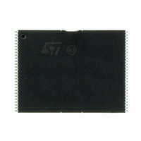
M29W640GH70NB6E NUMONYX, M29W640GH70NB6E Datasheet - Page 7

M29W640GH70NB6E
Manufacturer Part Number
M29W640GH70NB6E
Description
IC FLASH 64MBIT 70NS 56TSOP
Manufacturer
NUMONYX
Series
Axcell™r
Datasheet
1.M29W640GH70NB6E.pdf
(90 pages)
Specifications of M29W640GH70NB6E
Format - Memory
FLASH
Memory Type
FLASH - Nor
Memory Size
64M (8Mx8, 4Mx16)
Speed
70ns
Interface
Parallel
Voltage - Supply
2.7 V ~ 3.6 V
Operating Temperature
-40°C ~ 85°C
Package / Case
56-TSOP
Lead Free Status / RoHS Status
Lead free / RoHS Compliant
Available stocks
Company
Part Number
Manufacturer
Quantity
Price
1
Description
The M29W640G is a 64-Mbit (8 Mbit x8 or 4 Mbit x16) non-volatile memory that can be
read, erased and reprogrammed. These operations can be performed using a single low
voltage (2.7 to 3.6V) supply. On power-up the memory defaults to its read mode.
The memory is divided into blocks that can be erased independently so it is possible to
preserve valid data while old data is erased. Program and erase commands are written to
the command interface of the memory. An on-chip program/erase controller simplifies the
process of programming or erasing the memory by taking care of all of the special
operations that are required to update the memory contents. The end of a program or erase
operation can be detected and any error conditions identified. The command set required to
control the memory is consistent with JEDEC standards.
The M29W640GH and M29W640GL memory array is organized into 128 uniform blocks of
64 Kbytes each (or 32 Kwords each).
The M29W640GT and M29W640GB feature an asymmetric block architecture. The devices
have an array of 135 blocks, divided into 8 parameter blocks of 8 Kbytes each (or 4 Kwords
each), and 127 main blocks of 64 Kbytes each (or 32 Kwords each). The M29W640GT has
the parameter blocks at the top of the memory address space while the M29W640GB
locates the parameter blocks starting from the bottom.
Blocks are protected by groups to prevent accidental program or erase commands from
modifying the memory.
The M29W640G support asynchronous random read and page read from all blocks of the
memory array.
Chip Enable, Output Enable and Write Enable signals control the bus operation of the
memory. They allow simple connection to most microprocessors, often without additional
logic.
The V
program/erase operation can be obtained by holding V
The devices feature a full set of fast program commands to improve the programming
throughput:
Table
Table
M29W640GB.
On the M29W640GH and M29W640GL, the last and the first block is protected,
respectively.
On the M29W640GT and M29W640GB, the last two and the first two boot blocks are
protected.
2-byte program: it is not necessary to raise V
command
2-words/4-byte program: it is not necessary to raise V
command.
4-word/8-byte program: V
write to buffer and program, allowing to program in one shot a buffer of 16 words/32
bytes.
PP
/WP signal is used to enable faster programming of the device. Protection from
3, describes the protection granularity on the M29W640GH and M29W640GL.
4, and
Table
5. describe the protection granularity on the M29W640GT and
PP
/WP must be raised to 12 V before issuing this command.
PP
/WP to 12 V before issuing this
PP
/WP to V
PP
/WP to 12 V before issuing this
SS
:
7/90


