M27C256B-12F6 STMicroelectronics, M27C256B-12F6 Datasheet - Page 9
M27C256B-12F6
Manufacturer Part Number
M27C256B-12F6
Description
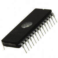
IC EPROM 256KBIT 120NS 28CDIP
Manufacturer
STMicroelectronics
Datasheet
1.M27C256B-15F1.pdf
(24 pages)
Specifications of M27C256B-12F6
Format - Memory
EPROMs
Memory Type
UV EPROM
Memory Size
256K (32K x 8)
Speed
120ns
Interface
Parallel
Voltage - Supply
4.5 V ~ 5.5 V
Operating Temperature
-40°C ~ 85°C
Package / Case
28-CDIP (0.600", 15.24mm) Window
Capacitance, Input
6 pF
Capacitance, Output
12 pF
Current, Input, Leakage
±10 μA (Read)
Current, Operating
30 mA (Read)
Current, Output, Leakage
±10 μA (Read)
Current, Supply
30 mA
Density
256K
Organization
32K×8
Package Type
FDIP28W
Temperature, Operating
-40 to +85 °C
Temperature, Operating, Maximum
85 °C
Temperature, Operating, Minimum
-40 °C
Time, Access
120 ns
Time, Fall
≤20 ns
Time, Programmable
100 μA
Time, Rise
≤20 ns
Voltage, Input, High
6 V (Read)
Voltage, Input, High Level
2 V (Min.)
Voltage, Input, Low
0.8 V (Read)
Voltage, Input, Low Level
0.8 V (Typ.)
Voltage, Output, High
4.3 V (Read)
Voltage, Output, Low
0.4 V (Read)
Voltage, Programmable
12.75 V ± 0.25 V
Voltage, Supply
5 V
Lead Free Status / RoHS Status
Lead free / RoHS Compliant
Other names
497-1647-5
Available stocks
Company
Part Number
Manufacturer
Quantity
Price
Company:

Part Number:
M27C256B-12F6
Manufacturer:
TI
Quantity:
4 350
Part Number:
M27C256B-12F6
Manufacturer:
ST
Quantity:
20 000
Company:
Part Number:
M27C256B-12F6L
Manufacturer:
Lattice
Quantity:
150
Part Number:
M27C256B-12F6L
Manufacturer:
ST
Quantity:
20 000


M27C256B
2.4
2.5
2.6
System considerations
The power switching characteristics of Advance CMOS EPROMs require careful decoupling
of the devices. The supply current, I
designer: the standby current level, the active current level, and transient current peaks that
are produced by the falling and rising edges of E. The magnitude of this transient current
peaks is dependent on the capacitive and inductive loading of the device at the output. The
associated transient voltage peaks can be suppressed by complying with the two line output
control and by properly selected decoupling capacitors. It is recommended that a 0.1µF
ceramic capacitor be used on every device between V
frequency capacitor of low inherent inductance and should be placed as close to the device
as possible. In addition, a 4.7µF bulk electrolytic capacitor should be used between V
V
connection point. The purpose of the bulk capacitor is to overcome the voltage drop caused
by the inductive effects of PCB traces.
Programming
When delivered (and after each erasure for UV EPROM), all bits of the M27C256B are in the
"1" state. Data is introduced by selectively programming "0"s into the desired bit locations.
Although only "0"s will be programmed, both "1"s and "0"s can be present in the data word.
The only way to change a '0' to a '1' is by die exposure to ultraviolet light (UV EPROM). The
M27C256B is in the programming mode when V
pulsed to V
pins. The levels required for the address and data inputs are TTL. V
6.25V ± 0.25 V.
PRESTO II programming algorithm
PRESTO II Programming Algorithm allows to program the whole array with a guaranteed
margin, in a typical time of 3.5 seconds. Programming with PRESTO II involves the
application of a sequence of 100µs program pulses to each byte until a correct verify occurs
(see
automatically activated in order to guarantee that each cell is programmed with enough
margin. No overprogram pulse is applied since the verify in MARGIN MODE provides
necessary margin to each programmed cell.
SS
for every eight devices. The bulk capacitor should be located near the power supply
Figure
IL
4.). During programming and verify operation, a MARGIN MODE circuit is
. The data to be programmed is applied to 8 bits in parallel to the data output
CC
, has three segments that are of interest to the system
PP
input is at 12.75V, G is at V
CC
and V
SS
. This should be a high
CC
is specified to be
Device operation
IH
and E is
CC
and
9/24
Related parts for M27C256B-12F6
Image
Part Number
Description
Manufacturer
Datasheet
Request
R

Part Number:
Description:
Manufacturer:
STMicroelectronics
Datasheet:
Part Number:
Description:
CMOS 256K (32K x 8) UV EPROM and OTP ROM
Manufacturer:
STMicroelectronics
Part Number:
Description:
Manufacturer:
STMicroelectronics
Datasheet:

Part Number:
Description:
IC EPROM 256KBIT 150NS 28CDIP
Manufacturer:
STMicroelectronics
Datasheet:

Part Number:
Description:
IC EPROM 256KBIT 90NS 28CDIP
Manufacturer:
STMicroelectronics
Datasheet:

Part Number:
Description:
IC OTP 256KBIT 150NS 32PLCC
Manufacturer:
STMicroelectronics
Datasheet:
Part Number:
Description:
IC OTP 256KBIT 70NS 32PLCC
Manufacturer:
STMicroelectronics
Datasheet:
Part Number:
Description:
IC OTP 256KBIT 100NS 32PLCC
Manufacturer:
STMicroelectronics
Datasheet:
Part Number:
Description:
IC EPROM 256KBIT 70NS 28CDIP
Manufacturer:
STMicroelectronics
Datasheet:

Part Number:
Description:
IC EPROM 256KBIT 100NS 28CDIP
Manufacturer:
STMicroelectronics
Datasheet:

Part Number:
Description:
IC EPROM 256KBIT 120NS 28CDIP
Manufacturer:
STMicroelectronics
Datasheet:
Part Number:
Description:
IC OTP 256KBIT 120NS 32PLCC
Manufacturer:
STMicroelectronics
Datasheet: