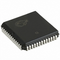
CY7C135-15JXC Cypress Semiconductor Corp, CY7C135-15JXC Datasheet

CY7C135-15JXC
Specifications of CY7C135-15JXC
Available stocks
Related parts for CY7C135-15JXC
CY7C135-15JXC Summary of contents
Page 1
... Each port has independent control pins: chip enable (CE), read or write enable (R/W), and output enable (OE). The CY7C135/135A is suited for those systems that do not require on-chip arbitration or are intolerant of wait states. Therefore, the user must be aware that simultaneous access to a location is possible ...
Page 2
... Selection Guide Parameter Maximum Access Time Maximum Operating Current Commercial Maximum Standby Current for Commercial I SB1 Pin Configurations Figure 1. Pin Diagram - CY7C135/135A (Top View 7C135/135A Pin Definitions Left Port Right Port A A Address Lines 0L–11L 0R–11R CE CE Chip Enable ...
Page 3
... V IN One Port CE or Com’l L ≥ – 0.2V Ind. ≥V V – 0. ≤ 0.2V Active Port Outputs, [ MAX CY7C135, CY7C135A CY7C1342 [3] .........................................–3.0V to +7.0V Ambient V CC Temperature ° ° + ± 10% ° ° – + ± 10% 7C135-25 7C135-15 7C135-20 7C135A-25 7C1342-15 7C1342-20 7C1342-25 Unit ...
Page 4
... CC Figure 3. AC Test Loads and Waveforms R = 250Ω TH OUTPUT 1.4V TH (b) Thévenin Equivalent (Load 1) ALL INPUT PULSES 3.0V 90% 90% 10% 10% GND ≤ CY7C135, CY7C135A CY7C1342 7C135-35 7C135-55 7C1342-35 7C1342-55 Unit Min Max Min Max 2.4 2.4 V 0.4 0.4 V 2.2 2.2 V ...
Page 5
... Document #: 38-06038 Rev. *D [6] 7C135-25 7C135-15 7C135-20 7C135A-25 7C1342-15 7C1342-20 7C1342-25 Min Max Min Max Min Max less than t and t is less than t HZCE LZCE HZOE Figure 6. CY7C135, CY7C135A CY7C1342 7C135-35 7C135-55 7C1342-35 7C1342-55 Unit Min Max Min Max LZOE Page [+] Feedback ...
Page 6
... Either Port Address Access [12,14] Figure 5. Read Cycle No. 2 Either Port CE/OE Access t ACE t DOE DATA VALID Figure 6. Read Timing with Port-to-Port t wc MATCH t PWE t SD VALID MATCH t WDD . IL CY7C135, CY7C135A CY7C1342 DATA VALID t HZCE t HZOE t PD [15 DDD VALID Page [+] Feedback ...
Page 7
... Data I/O pins enter high impedance when OE is held LOW during write. Document #: 38-06038 Rev SCE PWE t SD DATA VALID HIGH IMPEDANCE SCE PWE t SD DATA VALID t HZWE HIGH IMPEDANCE or (t PWE . CY7C135, CY7C135A CY7C1342 [16, 17, 18 LZOE [17, 19 LZWE + allow the I/O drivers to turn off and data HZWE SD Page [+] Feedback ...
Page 8
... SPS Document #: 38-06038 Rev VALID ADDRESS SCE t SOP t SD DATA VALID PWE t t SWRD DOE t SOP WRITE CYCLE READ CYCLE MATCH t SPS MATCH = CE = HIGH CY7C135, CY7C135A CY7C1342 [20] t OHA t ACE DATA VALID OUT [21, 22, 23] Page [+] Feedback ...
Page 9
... Architecture The CY7C135/135A consists of an array of 4K words of 8 bits each of dual-port RAM cells, I/O and address lines, and control signals (CE, OE, R/W). Two semaphore control pins exist for the CY7C1342 (SEM ). L/R Functional Description Write Operation Data must be set up for a duration R/W to guarantee a valid write ...
Page 10
... AMBIENT TEMPERATURE (°C) TYPICAL ACCESS TIME CHANGE vs. OUTPUT LOADING 20.0 15.0 10 4. 25° 200 400 600 800 1000 CAPACITANCE (pF) CY7C135, CY7C135A CY7C1342 OUTPUT SOURCE CURRENT vs. OUTPUT VOLTAGE 140 120 100 5. 25° 1.0 2.0 3.0 4.0 5.0 OUTPUT VOLTAGE (V) OUTPUT SINK CURRENT vs ...
Page 11
... Ordering Information 4K x8 Dual-Port SRAM Speed (ns) Ordering Code 15 CY7C135–15JC CY7C135-15JXC 20 CY7C135–20JC 25 CY7C135–25JC CY7C135-25JXC CY7C135A–25JI CY7C135–25JXI 35 CY7C135–35JC CY7C135–35JI 55 CY7C135–55JC CY7C135–55JI Package Diagram Figure 11. 52-Pin Pb-Free Plastic Leaded Chip Carrier J69 Document #: 38-06038 Rev. *D ...
Page 12
... Change from Spec number: 38-00541 to 38-06038 Power up requirements added to Maximum Ratings Information Removed cross information from features section Added Pb-Free Logo Added Pb-Free parts to ordering information: CY7C135-15JXC, CY7C135-25JXC Added CY7C135A parts Removed CY7C1342 from the ordering information table PSoC Solutions General psoc ...


