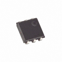
DS2430AP+ Maxim Integrated Products, DS2430AP+ Datasheet

DS2430AP+
Specifications of DS2430AP+
Related parts for DS2430AP+
DS2430AP+ Summary of contents
Page 1
... ORDERING INFORMATION DS2430A+ TO-92 Package DS2430AP+ 6-pin TSOC Package DS2430A+T&R TO-92 Package, Tape & Reel DS2430AP+T&R TSOC Package, Tape & Reel +Denotes a lead(Pb)-free/RoHS-compliant package. Contact factory for availability of the UCSP version. 256-Bit 1-Wire EEPROM PIN ASSIGNMENT ...
Page 2
... After the 48 bit of the serial number has been entered, the shift register contains the CRC value. Shifting in the 8 bits of CRC should return the shift register to all 0s. 1-Wire and iButton are registered trademarks of Maxim Integrated Products, Inc. ® communication line. Data is ...
Page 3
DS2430A BLOCK DIAGRAM Figure DS2430A ...
Page 4
HIERARCHICAL STRUCTURE FOR 1-WIRE PROTOCOL Figure 2 64-BIT LASERED ROM Figure 3 8-Bit CRC Code MSB LSB MSB 1-WIRE CRC GENERATOR Figure 4 48-Bit Serial Number LSB MSB Polynomial = ...
Page 5
... After issuing the Write Scratchpad command, the master must first provide a 1-byte address, followed by the data to be written to the scratchpad for the data memory. The DS2430A automatically increments the address after every byte it receives. After having received a data byte for address 1Fh, the address counter wraps around to 00h for the next byte and writing continues until the master sends a Reset Pulse ...
Page 6
... V READ MEMORY [F0h] The Read Memory command is used to read a portion or all of the EEPROM data memory and to copy the entire data memory into the scratchpad to prepare for changing a few bytes. To copy data from the data memory to the scratchpad and to read it, the master must issue the read memory command followed by the 1-byte starting address of the data to be read from the scratchpad ...
Page 7
... MEMORY FUNCTION FLOW CHART Figure 6 (cont’d) WRITE APPLICATION REGISTER [99h] This command is essentially the same as the Write Scratchpad command, but it addresses the 64-bit register scratchpad. After issuing the command code, the master must provide a 1-byte address, followed by the data to be written. The DS2430A automatically increments the address after every byte it receives. ...
Page 8
... MEMORY FUNCTION FLOW CHART Figure 6 (cont’d) READ APPLICATION REGISTER [C3h] This command is used to read the application register or the register scratchpad. As long as the application register is not yet locked, the DS2430A transmits data from the register scratchpad. After the application register is locked the DS2430A transmits data from the application register, making the register scratchpad inaccessible for reading ...
Page 9
BUS SYSTEM The 1-Wire bus is a system that has a single bus master and one or more slaves. In all instances, the DS2430A is a slave device. The bus master is typically a microcontroller. The discussion of this ...
Page 10
ROM FUNCTIONS FLOW CHART Figure DS2430A ...
Page 11
... This command can save time in a single-drop bus system by allowing the bus master to access the memory functions without providing the 64-bit ROM code. If more than one slave is present on the bus and a read command is issued following the Skip ROM command, data collision will occur on the bus as multiple slaves transmit simultaneously (open drain pulldowns produces a wired-AND result) ...
Page 12
... Figure 9 shows the initialization sequence required to begin any communication with the DS2430A. A Reset Pulse followed by a Presence Pulse indicates the DS2430A is ready to receive data, given the correct ROM and memory function command. If the bus master uses slew-rate control on the falling edge, it must pull down the line for t After the bus master has released the line it goes into Receive mode ...
Page 13
Master-to-Slave For a Write-1 time slot, the voltage on the data line must have crossed the V Write-1 low time t is expired. For a Write-0 time slot, the voltage on the data line must stay below W1LMAX the V ...
Page 14
Slave-to-Master A Read-data time slot begins like a Write-1 time slot. The voltage on the data line must remain below V until the read low time DS2430A starts pulling the data line low; its internal timing generator ...
Page 15
... MEMORY FUNCTION EXAMPLE Example: Write 2 data bytes to data memory locations 0006h and 0007h. Read entire data memory. MASTER MODE DATA (LSB FIRST) TX Reset RX Presence <2 Data Bytes> TX Reset RX Presence <2 Data Bytes> TX Reset RX Presence <Data Line High> TX Reset RX Presence <32 Bytes> ...
Page 16
ABSOLUTE MAXIMUM RATINGS Voltage on DATA to Ground DATA Sink Current Operating Temperature Range Junction Temperature Storage Temperature Range Lead Temperature (soldering 10s) Soldering Temperature (reflow) Stresses beyond those listed under “Absolute Maximum Ratings” may cause permanent damage to the ...
Page 17
PARAMETER SYMBOL EEPROM Programming Current I PROG Programming Time t PROG Write/Erase Cycles (En durance) (Notes 20, 21) Data Retention (Notes 22 23, 24) = -40°C are guaranteed by design only and not production-tested. Note 1: ...
Page 18
Package Information For the latest package outline information and land patterns www.maxim-ic.com/packages. Note that a “+”, “#”, or “-“ in the package code indicates RoHS status only. Package drawings may show a different suffix character, but the drawing ...
Page 19
... Maxim/Dallas Semiconductor cannot assume responsibility for use of any circuitry other than circuitry entirely embodied in a Maxim/Dallas Semiconductor product. No circuit patent licenses are implied. Maxim/Dallas Semiconductor reserves the right to change the circuitry and The Maxim logo is a registered trademark of Maxim Integrated Products, Inc. DESCRIPTION ILMAX Note 6 ...


