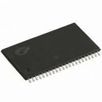
CY62147EV30LL-55ZSXE Cypress Semiconductor Corp, CY62147EV30LL-55ZSXE Datasheet - Page 4

CY62147EV30LL-55ZSXE
Manufacturer Part Number
CY62147EV30LL-55ZSXE
Description
IC SRAM 4MBIT 55NS 44TSOP
Manufacturer
Cypress Semiconductor Corp
Type
Asynchronousr
Datasheet
1.CY62147EV30LL-45ZSXI.pdf
(16 pages)
Specifications of CY62147EV30LL-55ZSXE
Memory Size
4M (256K x 16)
Package / Case
44-TSOP II
Format - Memory
RAM
Memory Type
SRAM
Speed
55ns
Interface
Parallel
Voltage - Supply
2.2 V ~ 3.6 V
Operating Temperature
-40°C ~ 125°C
Access Time
55 ns
Supply Voltage (max)
3.6 V
Supply Voltage (min)
2.2 V
Maximum Operating Current
25 mA
Maximum Operating Temperature
+ 125 C
Minimum Operating Temperature
- 40 C
Mounting Style
SMD/SMT
Number Of Ports
1
Operating Supply Voltage
3 V
Lead Free Status / RoHS Status
Lead free / RoHS Compliant
Lead Free Status / RoHS Status
Lead free / RoHS Compliant, Lead free / RoHS Compliant
Maximum Ratings
Exceeding the maximum ratings may impair the useful life of the
device. User guidelines are not tested.
Storage temperature ............................... –65 °C to + 150 °C
Ambient temperature with
power applied ......................................... –55 °C to + 125 °C
Supply voltage to ground
potential .......................... –0.3 V to + 3.9 V (V
DC voltage applied to outputs
in High Z state
Electrical Characteristics
Over the Operating Range
Capacitance
For all packages.
Notes
Document Number: 38-05440 Rev. *J
V
V
V
V
I
I
I
I
I
C
C
5. V
6. V
7. Full device AC operation assumes a minimum of 100 s ramp time from 0 to V
8. Typical values are included for reference only and are not guaranteed or tested. Typical values are measured at V
9. Chip enable (CE) and byte enables (BHE and BLE) need to be tied to CMOS levels to meet the I
10. Tested initially and after any design or process changes that may affect these parameters.
Parameter
IX
OZ
CC
SB1
SB2
OH
OL
IH
IL
IN
OUT
IL(min)
IH(max)
[9]
Parameter
= –2.0 V for pulse durations less than 20 ns.
= V
CC
Output HIGH
voltage
Output LOW
voltage
Input HIGH
voltage
Input LOW
voltage
Input leakage
current
Output leakage
current
V
supply current
Automatic CE
power-down
current — CMOS
inputs
Automatic CE
power-down
current — CMOS
inputs
CC
[5, 6]
+ 0.75 V for pulse durations less than 20 ns.
Description
[10]
operating
.............. –0.3 V to 3.9 V (V
Input capacitance
Output capacitance
I
I
I
I
V
V
V
V
GND < V
GND < V
f = f
f = 1 MHz
CE > V
V
f = f
V
CE > V
V
f = 0, V
OH
OH
OL
OL
f = 0 (OE, BHE, BLE and WE),
CC
CC
CC
CC
IN
CC
IN
= 0.1 mA
= 2.1 mA, V
max
max
= –0.1 mA
= –1.0 mA, V
> V
> V
= 2.7 V to 3.6 V
= 2.7 V to 3.6 V
= 2.2 V to 2.7 V
= 2.2 V to 2.7 V
= 3.60 V
Description
CC
CC
CC
CC
CC
= 1/t
(address and data only),
I
O
Test Conditions
< V
– 0.2 V
– 0.2 V
= 3.60 V
< V
– 0.2 V, V
– 0.2 V or V
RC
CC
CC
CCmax
CCmax
CC
, output disabled
V
I
CMOS levels
CC
OUT
CC
= 2.70 V
> 2.70 V
IN
+ 0.3 V)
+ 0.3 V)
= V
= 0 mA
IN
< 0.2 V
CC(max)
< 0.2 V,
T
V
A
CC
= 25 °C, f = 1 MHz,
= V
CC
(min) and 200 s wait time after V
CC(typ)
DC input voltage
Output current into outputs (LOW) ............................. 20 mA
Static discharge voltage .......................................... >2001 V
(MIL-STD-883, method 3015)
Latch-up current ...................................................... >200 mA
Operating Range
Test Conditions
CY62147EV30LL Industrial –40 °C to +85 °C 2.2 V to 3.6 V
–0.3
–0.3
Min
2.0
2.4
1.8
2.2
–1
–1
Device
–
–
–
–
–
–
SB2
/ I
45 ns (Industrial)
CCDR
[5, 6]
Typ
spec. Other inputs can be left floating.
........... –0.3 V to 3.9 V (V
15
Range
–
–
–
–
–
–
–
–
–
–
2
1
1
[8]
CC
CC
= V
CY62147EV30 MoBL
stabilization.
CC(typ)
Max
Temperature
10
10
, T
V
V
Ambient
A
CC
CC
Max
0.4
0.4
0.6
0.8
2.5
= 25 °C.
+1
+1
20
–
–
7
7
+ 0.3
+ 0.3
CCmax
Page 4 of 16
Unit
+ 0.3 V)
pF
pF
V
Unit
mA
A
A
A
A
CC
V
V
V
V
V
V
V
V
[7]
®
[+] Feedback


