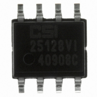
CAT25128VI-G ON Semiconductor, CAT25128VI-G Datasheet - Page 3

CAT25128VI-G
Manufacturer Part Number
CAT25128VI-G
Description
IC EEPROM 128KBIT 10MHZ 8SOIC
Manufacturer
ON Semiconductor
Datasheet
1.CAT25128VI-G.pdf
(16 pages)
Specifications of CAT25128VI-G
Format - Memory
EEPROMs - Serial
Memory Type
EEPROM
Memory Size
128K (16K x 8)
Speed
10MHz
Interface
SPI, 3-Wire Serial
Voltage - Supply
1.8 V ~ 5.5 V
Operating Temperature
-40°C ~ 85°C
Package / Case
8-SOIC (3.9mm Width)
Density
128Kb
Interface Type
Serial (SPI)
Organization
16Kx8
Access Time (max)
75ns
Frequency (max)
5MHz
Write Protection
Yes
Data Retention
100Year
Operating Supply Voltage (typ)
2.5/3.3/5V
Operating Temp Range
-40C to 85C
Supply Current
4mA
Operating Supply Voltage (min)
1.8V
Operating Supply Voltage (max)
5.5V
Operating Temperature Classification
Industrial
Mounting
Surface Mount
Pin Count
8
Maximum Clock Frequency
10 MHz
Access Time
75 ns
Supply Voltage (max)
5.5 V
Supply Voltage (min)
1.8 V
Maximum Operating Current
4 mA
Maximum Operating Temperature
+ 85 C
Mounting Style
SMD/SMT
Minimum Operating Temperature
- 40 C
Operating Supply Voltage
2.5 V, 3.3 V, 5 V
Lead Free Status / RoHS Status
Lead free / RoHS Compliant
Available stocks
Company
Part Number
Manufacturer
Quantity
Price
Company:
Part Number:
CAT25128VI-GT3
Manufacturer:
ON Semiconductor
Quantity:
5 700
Part Number:
CAT25128VI-GT3
Manufacturer:
ON/安森美
Quantity:
20 000
4. AC Test Conditions:
5. This parameter is tested initially and after a design or process change that affects the parameter.
6. t
7. All Chip Select (CS) timing parameters are defined relative to the positive clock edge (Figure 2). t
8. t
Table 5. A.C. CHARACTERISTICS
Table 6. POWER−UP TIMING
for die revision D and higher. The die revision D is identified by letter “D” or a dedicated marking code on top of the package. For
previous product revision (Rev.C) the t
t
WC
PUR
t
t
WC
RI
FI
Symbol
Symbol
Input Pulse Voltages: 0.3 V
Input rise and fall times: ≤ 10 ns
Input and output reference voltages: 0.5 V
Output load: current source I
(Note 5)
(Note 5)
t
t
is the time from the rising edge of CS after a valid write sequence to the end of the internal write cycle.
t
f
t
t
t
t
t
t
t
WPH
(Note 6)
PUW
t
t
CNH
WPS
SCK
t
t
t
t
t
CSS
CSH
CNS
PUR
and t
t
WH
DIS
SU
t
WL
HD
CD
HO
t
HZ
CS
LZ
H
V
PUW
are the delays required from the time V
HOLD to Output Low Z
HOLD Setup Time
HOLD Hold Time
HOLD to Output High Z
CS High Time
CS Setup Time
CS Hold Time
CS Inactive Setup Time
CS Inactive Hold Time
WP Setup Time
WP Hold Time
Clock Frequency
Data Setup Time
Data Hold Time
SCK High Time
SCK Low Time
Input Rise Time
Input Fall Time
Output Valid from Clock Low
Output Hold Time
Output Disable Time
Write Cycle Time
Power−up to Read Operation
Power−up to Write Operation
Parameter
CC
OL max
(Notes 5, 8)
to 0.7 V
(T
/I
OH max
A
CC
CSH
= −40°C to +85°C (Industrial) and T
CC
is defined relative to the negative clock edge.
; C
L
= 50 pF
CC
Parameter
V
V
http://onsemi.com
CC
CC
is stable until the specified operation can be initiated.
= 2.5 V − 5.5 V / −405C to +1255C
= 1.8 V − 5.5 V / −405C to +855C
Min
140
100
DC
40
40
75
75
10
30
30
20
20
10
0
0
3
A
= −40°C to +125°C (Extended).) (Notes 4, 7)
Max
100
50
75
50
5
2
2
5
V
Min
DC
CSH
CC
20
20
40
40
10
70
15
15
15
15
10
60
−405C to +855C
0
0
= 2.5 V − 5.5 V
timing specification is valid
Max
1
1
Max
10
25
40
20
25
2
2
5
Units
ms
ms
Units
MHz
ms
ns
ns
ns
ns
ns
ms
ms
ns
ns
ns
ns
ns
ns
ns
ns
ns
ns
ns
ns
ns


