AT24C01B-TH-T Atmel, AT24C01B-TH-T Datasheet
AT24C01B-TH-T
Specifications of AT24C01B-TH-T
Available stocks


Related parts for AT24C01B-TH-T


AT24C01B-TH-T Summary of contents
Page 1
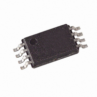
... The AT24C01B is available in space-saving 8-lead PDIP, 8-lead JEDEC SOIC, 8-lead Ultra Thin Mini-MAP (MLP 2x3) SOT23, 8-lead TSSOP, and 8-ball dBGA2 packages and is accessed via a Two-wire serial interface. In addition, the AT24C01B is available in 1.8V (1.8V to 5.5V) version. Table 0-1. Pin Configuration ...
Page 2
... Voltage on Any Pin with Respect to Ground .................................... –1.0V to +7.0V Maximum Operating Voltage .......................................... 6.25V DC Output Current........................................................ 5.0 mA Figure 0-1. Block Diagram VCC GND WP SCL SDA AT24C01B 2 *NOTICE: START STOP LOGIC SERIAL CONTROL LOGIC LOAD COMP DEVICE ADDRESS LOAD COMPARATOR R/W DATA WORD ADDR/COUNTER Y DEC ...
Page 3
... DEVICE/PAGE ADDRESSES (A2, A1, A0): The A2, A1 and A0 pins are device address inputs that are hard wired for the AT24C01B. As many as eight 1K devices may be addressed on a sin- gle bus system (device addressing is discussed in detail under the Device Addressing section). WRITE PROTECT (WP): The AT24C01B has a write protect pin that provides hardware data protection ...
Page 4
... IH V Output Low Level V = 3.0V OL2 CC V Output Low Level V = 1.8V OL1 CC Note min and V max are reference only and are not tested AT24C01B 4 = 25° 1.0 MHz SCL 40°C to +85°C, V – AI Test Condition READ at 100 kHz WRITE at 100 kHz ...
Page 5
Table 2-3. AC Characteristics Applicable over recommended operating range from T 100 pF (unless otherwise noted) Symbol Parameter f Clock Frequency, SCL SCL t Clock Pulse Width Low LOW t Clock Pulse Width High HIGH t Noise Suppression Time I ...
Page 6
... EEPROM in 8-bit words. The EEPROM sends a zero to acknowledge that it has received each word. This happens during the ninth clock cycle. STANDBY MODE: The AT24C01B features a low-power standby mode which is enabled: (a) upon power-up and (b) after the receipt of the STOP bit and the completion of any internal operations ...
Page 7
Bus Timing Figure 4-1. SCL: Serial Clock, SDA: Serial Data I/O SCL t SU.STA SDA IN SDA OUT 5. Write Cycle Timing Figure 5-1. SCL: Serial Clock, SDA: Serial Data I/O SCL SDA 8th BIT WORDn Note: 1. The ...
Page 8
... Figure 5-2. Data Validity SDA SCL Figure 5-3. Start and Stop Definition SDA SCL Figure 5-4. Output Acknowledge SCL DATA IN DATA OUT AT24C01B 8 DATA STABLE DATA STABLE DATA CHANGE START 1 START STOP 8 9 ACKNOWLEDGE 5156E–SEEPR–10/08 ...
Page 9
... The data word address lower three bits are internally incremented following the receipt of each data word. The higher data word address bits are not incremented, retaining the memory page row location. When the word address, internally generated, reaches the page boundary, the fol- lowing byte is placed at the beginning of the same page. If more than eight data words are transmitted to the EEPROM, the data word address will “ ...
Page 10
... The sequential read operation is terminated when the microcontroller does not respond with a zero but does generate a following stop condition (see Figure 8-1. Device Address Figure 8-2. Byte Write AT24C01B 10 Figure 8-5 on page 11). Figure 8-6 on page 1K * Figure 8-4 on 12) ...
Page 11
Figure 8-3. Page Write * = ( Don’t Care Bit) Figure 8-4. Current Address Read Figure 8-5. Random Read (* = Don’t Care Bit) 5156E–SEEPR–10/ ...
Page 12
... Figure 8-6. Sequential Read AT24C01B 12 5156E–SEEPR–10/08 ...
Page 13
... AT24C01B Ordering Information Ordering Code AT24C01B-PU (Bulk form only) (1) AT24C01BN-SH-B (NiPdAu Lead Finish) (2) AT24C01BN-SH-T (NiPdAu Lead Finish) (1) AT24C01B-TH-B (NiPdAu Lead Finish) (2) AT24C01B-TH-T (NiPdAu Lead Finish) -T(2) AT24C01BY6-YH (NiPdAu Lead Finish) -T(2) AT24C01B-TSU -T(2) AT24C01BU3-UU (3) AT24C01B-W-11 Notes: 1. “-B” denotes bulk. 2. “-T” denotes tape and reel. SOIC = 4K per reel. TSSOP, Ultra Thin Mini MAP, SOT 23 and dBGA2 = 5K per reel. ...
Page 14
... Part Marking Scheme 8-PDIP Seal Year TOP MARK |---|---|---|---|---|---|---|---| A |---|---|---|---|---|---|---|---| 0 |---|---|---|---|---|---|---|---| * |---|---|---|---|---|---|---|---| | Pin 1 Indicator (Dot Material Set Y = Seal Year WW = Seal Week 01B = Device V = Voltage Indicator *Lot Number to Use ALL Characters in Marking BOTTOM MARK AT24C01B 14 | Seal Week | | Lot Number No Bottom Mark | W 5156E–SEEPR–10/08 ...
Page 15
TOP MARK |---|---|---|---|---|---|---|---| A |---|---|---|---|---|---|---|---| 0 |---|---|---|---|---|---|---|---| * |---|---|---|---|---|---|---|---| | Pin 1 Indicator (Dot Material Set Y = Seal Year WW = Seal Week 01B = Device 1 = Voltage Indicator *Lot Number to Use ALL Characters ...
Page 16
... BOTTOM MARK |---|---|---|---|---|---|---| |---|---|---|---|---|---|---| |---|---|---|---|---|---|---| Lot Number XX = Country of Origin AAAAAA = Lot Number SOT23 TOP MARK Line 1 -----------> Device 1 = Voltage Indicator W = Write Protect Feature U = Material Set BOTTOM MARK |---|---|---|---| Y |---|---|---|---| Y = One Digit Year Code M = Seal Month TC = Trace Code AT24C01B <- Pin 1 Indicator |---|---|---|---|---| |---|---|---|---|---| * | Pin 1 Indicator (Dot 5156E–SEEPR–10/08 ...
Page 17
ULTRA THIN MINI MAP TOP MARK Pin 1 Indicator (Dot) 01B = Device H = Material Set 1 = Voltage Indicator Y = Year of Assembly TC = Trace Code dBGA2 LINE 1-------> LINE 2-------> 01B = Device U = ...
Page 18
... D, D1 and E1 dimensions do not include mold Flash or protrusions. Mold Flash or protrusions shall not exceed 0.010 inch and eA measured with the leads constrained to be perpendicular to datum. 5. Pointed or rounded lead tips are preferred to ease insertion and b3 maximum dimensions do not include Dambar protrusions. Dambar protrusions shall not exceed 0.010 (0.25 mm). 2325 Orchard Parkway San Jose, CA 95131 R AT24C01B ...
Page 19
JEDEC SOIC e Side View Note: These drawings are for general information only. Refer to JEDEC Drawing MS-012, Variation AA for proper dimensions, tolerances, datums, etc. 1150 E. Cheyenne Mtn. Blvd. Colorado Springs, CO 80906 R 5156E–SEEPR–10/08 ...
Page 20
... Dimension b does not include Dambar protrusion. Allowable Dambar protrusion shall be 0.08 mm total in excess of the b dimension at maximum material condition. Dambar cannot be located on the lower radius of the foot. Minimum space between protrusion and adjacent lead is 0.07 mm. 5. Dimension D and determined at Datum Plane H. 2325 Orchard Parkway San Jose, CA 95131 R AT24C01B TITLE 8A2, 8-lead, 4 ...
Page 21
Mini Map D Notes: 1. This drawing is for general information only. Refer to JEDEC Drawing MO-229, for proper dimensions, tolerances, datums, etc. 2. Dimension b applies to metallized terminal and is measured between 0.15 mm and ...
Page 22
... The Dambar cannot be located on the lower radius of the foot. Minimum space between protrusion and an adjacent lead shall not be less than 0.07 mm. 1150 E. Cheyenne Mtn. Blvd. Colorado Springs, CO 80906 R AT24C01B Top View ...
Page 23
PIN 1 BALL PAD CORNER Top View PIN 1 BALL PAD CORNER 1 2 (d1 (e1) Bottom View 8 SOLDER BALLS 1. Dimension “b” is measured at the maximum solder ball diameter. ...
Page 24
... Revision History Doc. Rev. 5156E 5156D 5156C 5156B 5156A AT24C01B 24 Date Comments 10/2008 Modified Ordering Information 8/2007 Added Part Marking Scheme Removed NC and GND from Pin Configuration; Removed Preliminary from page 1 and all headers/footers; Added 2-wire 4/2007 Software Reset; Removed LSB and MSB from figures; Removed waffle pack from die sale order information Ordering information changed ...
Page 25
... Disclaimer: The information in this document is provided in connection with Atmel products. No license, express or implied, by estoppel or otherwise, to any intellectual property right is granted by this document or in connection with the sale of Atmel products. EXCEPT AS SET FORTH IN ATMEL’S TERMS AND CONDI- TIONS OF SALE LOCATED ON ATMEL’S WEB SITE, ATMEL ASSUMES NO LIABILITY WHATSOEVER AND DISCLAIMS ANY EXPRESS, IMPLIED OR STATUTORY WARRANTY RELATING TO ITS PRODUCTS INCLUDING, BUT NOT LIMITED TO, THE IMPLIED WARRANTY OF MERCHANTABILITY, FITNESS FOR A PARTICULAR PURPOSE, OR NON-INFRINGEMENT ...