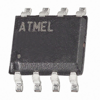
AT24HC02BN-SH-T Atmel, AT24HC02BN-SH-T Datasheet

AT24HC02BN-SH-T
Specifications of AT24HC02BN-SH-T
AT24HC02BN-10SU-1.8 SL383
Available stocks
Related parts for AT24HC02BN-SH-T
AT24HC02BN-SH-T Summary of contents
Page 1
... Description The AT24HC02B provides 2048 bits of serial electrically erasable and programmable read-only memory (EEPROM) organized as 256 words of 8 bits each. The device is optimized for use in many industrial and commercial applications where low-power and low-voltage operation are essential. The AT24HC02B is available in space-saving 8-lead PDIP, 8-lead JEDEC SOIC and 8-lead TSSOP packages and is accessed via a two-wire serial interface ...
Page 2
Absolute Maximum Ratings* Operating Temperature......................................−55°C to +125°C Storage Temperature .........................................−65°C to +150°C Voltage on Any Pin with Respect to Ground ........................................ −1.0V to +7.0V Maximum Operating Voltage .......................................... 6.25V DC Output Current........................................................ 5.0 mA Figure 2-1. AT24HC02B 2 *NOTICE: Block ...
Page 3
Pin Description SERIAL CLOCK (SCL): The SCL input is used to positive edge clock data into each EEPROM device and negative edge clock data out of each device. SERIAL DATA (SDA): The SDA pin is bidirectional for serial data ...
Page 4
... Memory Organization AT24HC02B, 2K SERIAL EEPROM: The 2K is internally organized with 32 pages of 8 bytes each. Random word addressing requires an 8-bit data word address. (1) Table 4-1. Pin Capacitance Applicable over recommended operating range from T Symbol Test Condition C Input/Output Capacitance (SDA) I/O C Input Capacitance (A ...
Page 5
Table 4-3. AC Characteristics Applicable over recommended operating range from T 100 pF (unless otherwise noted) Symbol Parameter f Clock Frequency, SCL SCL t Clock Pulse Width Low LOW t Clock Pulse Width High HIGH t Noise Suppression Time I ...
Page 6
Device Operation CLOCK and DATA TRANSITIONS: The SDA pin is normally pulled high with an external device. Data on the SDA pin may change only during SCL low time periods (see Data changes during SCL high periods will indicate ...
Page 7
SOFTWARE RESET: After an interruption in protocol, power loss or system reset, any two-wire part can be reset by following these steps: (a) Clock cycles, (b) Look for SDA high in each cycle while SCL is ...
Page 8
Figure 5-6. Output Acknowledge SCL DATA IN DATA OUT 6. Device Addressing The 2K EEPROM device requires an 8-bit device address word following a start condition to enable the chip for a read or write operation, as shown in Figure ...
Page 9
... The data word address lower three (2K) bits are internally incremented following the receipt of each data word. The higher data word address bits are not incremented, retaining the memory page row location. When the word address, internally generated, reaches the page boundary, the following byte is placed at the beginning of the same page. If more than eight (2K) data words are transmitted to the EEPROM, the data word address will “ ...
Page 10
... The address “roll over” during read is from the last byte of the last memory page to the first byte of the first page. The address “roll over” during write is from the last byte of the current page to the first byte of the same page. Once the device address with the read/write select bit set to “ ...
Page 11
... As long as the EEPROM receives an acknowledge, it will continue to increment the data word address and serially clock out sequential data words. When the memory address limit is reached, the data word address will “roll over” and the sequential read will continue. The sequential read operation is terminated when the microcontroller does not respond with a “ ...
Page 12
... AT24HC02B Ordering Information Ordering Code AT24HC02B-PU (Bulk form only) (1) AT24HC02BN-SH-B (NiPdAu Lead Finish) (2) AT24HC02BN-SH-T (NiPdAu Lead Finish) (1) AT24HC02B-TH-B (NiPdAu Lead Finish) (2) AT24HC02B-TH-T (NiPdAu Lead Finish) (3) AT24HC02B-W-11 Notes: 1. “-B” denotes bulk. 2. “-T” denotes tape and reel. SOIC = 4K per reel. TSSOP = 5K per reel. ...
Page 13
Part marking scheme 10.1 8-PDIP TOP MARK Seal Year |---|---|---|---|---|---|---|---| |---|---|---|---|---|---|---|---| |---|---|---|---|---|---|---|---| * Lot Number |---|---|---|---|---|---|---|---| | Pin 1 Indicator (Dot) 10.2 8-SOIC TOP MARK Seal Year |---|---|---|---|---|---|---|---| A T ...
Page 14
TOP MARK Pin 1 Indicator (Dot) | |---|---|---|---| * |---|---|---|---|---| |---|---|---|---|---| BOTTOM MARK |---|---|---|---|---|---|---| P H |---|---|---|---|---|---|---| |---|---|---|---|---|---|---| <- Pin 1 Indicator AT24HC02B SEAL ...
Page 15
Packaging Information 11.1 8P3 – PDIP Top View PLCS Side View Notes: 1. This drawing is for general information only; refer to JEDEC Drawing MS-001, Variation BA, for additional information. 2. Dimensions A and L ...
Page 16
JEDEC SOIC Top View e Side View Note: These drawings are for general information only. Refer to JEDEC Drawing MS-012, Variation AA for proper dimensions, tolerances, datums, etc. 1150 E. Cheyenne Mtn. Blvd. Colorado Springs, CO 80906 ...
Page 17
TSSOP Pin 1 indicator this corner N Top View Side View Notes: 1. This drawing is for general information only. Refer to JEDEC Drawing MO-153, Variation AA, for proper dimensions, tolerances, ...
Page 18
Revision History Doc. Rev. 5134E 5134D 5134C 5134B AT24HC02B 18 Date Comments Added part marking scheme 3/2008 Updated to new template Removed reference to Waffle Pack on page 1 Added lines to Ordering Code table 4/2007 Shrink Pin Diagram; ...
Page 19
... Disclaimer: The information in this document is provided in connection with Atmel products. No license, express or implied, by estoppel or otherwise, to any intellectual property right is granted by this document or in connection with the sale of Atmel products. EXCEPT AS SET FORTH IN ATMEL’S TERMS AND CONDI- TIONS OF SALE LOCATED ON ATMEL’S WEB SITE, ATMEL ASSUMES NO LIABILITY WHATSOEVER AND DISCLAIMS ANY EXPRESS, IMPLIED OR STATUTORY WARRANTY RELATING TO ITS PRODUCTS INCLUDING, BUT NOT LIMITED TO, THE IMPLIED WARRANTY OF MERCHANTABILITY, FITNESS FOR A PARTICULAR PURPOSE, OR NON-INFRINGEMENT ...


