24LCS52-I/ST Microchip Technology, 24LCS52-I/ST Datasheet - Page 11
24LCS52-I/ST
Manufacturer Part Number
24LCS52-I/ST
Description
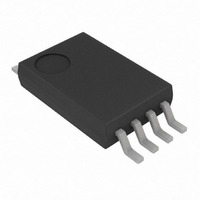
IC EEPROM 2KBIT 400KHZ 8TSSOP
Manufacturer
Microchip Technology
Datasheet
1.24AA52-ISN.pdf
(28 pages)
Specifications of 24LCS52-I/ST
Format - Memory
EEPROMs - Serial
Memory Type
EEPROM
Memory Size
2K (256 x 8)
Speed
100kHz, 400kHz
Interface
I²C, 2-Wire Serial
Voltage - Supply
2.2 V ~ 5.5 V
Operating Temperature
-40°C ~ 85°C
Package / Case
8-TSSOP
Lead Free Status / RoHS Status
Lead free / RoHS Compliant
Available stocks
Company
Part Number
Manufacturer
Quantity
Price
Company:

Part Number:
24LCS52-I/ST
Manufacturer:
MICROCHIP
Quantity:
12 000


7.0
Read operations are initiated in the same way as write
operations, with the exception that the R/W bit of the
slave address is set to ‘
of read operations: current address read, random read
and sequential read.
7.1
The 24XXX52 contains an address counter that
maintains the address of the last word accessed, inter-
nally incremented by ‘
access (either a read or write operation) was to
address
would access data from address
the slave address with R/W bit set to ‘
issues an acknowledge and transmits the 8-bit data
word. The master will not acknowledge the transfer, but
does generate a Stop condition and the 24XXX52
discontinues transmission (Figure 7-1).
7.2
Random read operations allow the master to access
any memory location in a random manner. To perform
this type of read operation, the word address must first
be set. This is done by sending the word address to the
24XXX52 as part of a write operation. Once the word
address is sent, the master generates a Start condition
following the acknowledge. This terminates the write
operation, but not before the internal Address Pointer is
set. The master then issues the control byte again, but
with the R/W bit set to a ‘
an acknowledge and transmits the 8-bit data word. The
master will not acknowledge the transfer, but does
generate a Stop condition and the 24XXX52
discontinues transmission (Figure 7-2).
FIGURE 7-1:
© 2005 Microchip Technology Inc.
READ OPERATION
Current Address Read
Random Read
n
, the next current address read operation
Bus Activity
Master
SDA Line
Bus Activity
CURRENT ADDRESS READ
1
1
’. There are three basic types
1
’. Therefore, if the previous
’. The 24XXX52 then issues
n+1
S
T
A
R
T
S
. Upon receipt of
1
’, the 24XXX52
Control
Byte
7.3
Sequential reads are initiated in the same way as a
random read, with the exception that after the 24XXX52
transmits the first data byte, the master issues an
acknowledge, as opposed to a Stop condition in a
random read. This directs the 24XXX52 to transmit the
next sequentially addressed 8-bit word (Figure 7-3).
To provide sequential reads, the 24XXX52 contains an
internal Address Pointer, which is incremented by one
at the completion of each operation. This Address
Pointer allows the entire memory contents to be serially
read during one operation.
7.4
The Chip Select bits (A2, A1, A0) can be used to
expand the contiguous address space for up to 16K bits
by adding up to eight 24XXX52 devices on the same
bus. In this case, software can use A0 of the control
byte as address bit A8; A1 as address bit A9, and A2
as address bit A10. It is not possible to sequentially
read across device boundaries.
7.5
The 24XXX52 employs a V
which disables the internal erase/write logic if the V
is below 1.5V at nominal conditions.
The SCL and SDA inputs have Schmitt Trigger and
filter circuits which suppress noise spikes to assure
proper device operation, even on a noisy bus.
A
C
K
24AA52/24LCS52
Sequential Read
Contiguous Addressing Across
Multiple Devices
Noise Protection and Brown-Out
Data (n)
CC
threshold detector circuit
N
O
C
A
K
P
S
T
O
P
DS21166J-page 11
CC
Related parts for 24LCS52-I/ST
Image
Part Number
Description
Manufacturer
Datasheet
Request
R

Part Number:
Description:
IC EEPROM 2KBIT 400KHZ 8SOIC
Manufacturer:
Microchip Technology
Datasheet:
Part Number:
Description:
IC,SERIAL EEPROM,256X8,CMOS,TSSOP,8PIN,PLASTIC
Manufacturer:
Microchip Technology
Datasheet:

Part Number:
Description:
2K 2.2V I2C� Serial EEPROM with Software Write-Protect
Manufacturer:
MICROCHIP [Microchip Technology]
Datasheet:
Part Number:
Description:
IC EEPROM 2KBIT 400KHZ 8SOIC
Manufacturer:
Microchip Technology
Datasheet:
Part Number:
Description:
IC EEPROM 2KBIT 400KHZ 8DIP
Manufacturer:
Microchip Technology
Datasheet:
Part Number:
Description:
IC EEPROM 2KBIT 400KHZ 8DIP
Manufacturer:
Microchip Technology
Datasheet:
Part Number:
Description:
IC,SERIAL EEPROM,256X8,CMOS,TSSOP,8PIN,PLASTIC
Manufacturer:
Microchip Technology
Datasheet:

Part Number:
Description:
2 2k 2.2v I C Serial Eeprom With Software Write-protect
Manufacturer:
Microchip Technology Inc.
Datasheet:
Part Number:
Description:
EEPROM 256x8 - 2.5V Industrial Temp
Manufacturer:
Microchip Technology
Part Number:
Description:
EEPROM 256x8 - 2.5V Lead Free Package
Manufacturer:
Microchip Technology
Part Number:
Description:
EEPROM 256x8 - 2.5V Industrial Temp
Manufacturer:
Microchip Technology
Part Number:
Description:
EEPROM 256x8 - 2.5V Lead Free Package
Manufacturer:
Microchip Technology
Part Number:
Description:
EEPROM 256x8 - 2.5V Lead Free Package
Manufacturer:
Microchip Technology
Part Number:
Description:
IC EEPROM 2KBIT 400KHZ 8DFN
Manufacturer:
Microchip Technology
Datasheet: