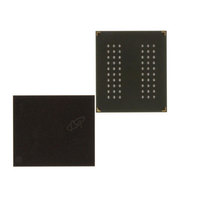
MT46H64M16LFCK-5 IT:A TR Micron Technology Inc, MT46H64M16LFCK-5 IT:A TR Datasheet - Page 48

MT46H64M16LFCK-5 IT:A TR
Manufacturer Part Number
MT46H64M16LFCK-5 IT:A TR
Description
IC DDR SDRAM 1GBIT 60VFBGA
Manufacturer
Micron Technology Inc
Datasheet
1.MT46H64M16LFCK-5A_TR.pdf
(95 pages)
Specifications of MT46H64M16LFCK-5 IT:A TR
Format - Memory
RAM
Memory Type
Mobile DDR SDRAM
Memory Size
1G (64M x 16)
Speed
200MHz
Interface
Parallel
Voltage - Supply
1.7 V ~ 1.95 V
Operating Temperature
-40°C ~ 85°C
Package / Case
60-VFBGA
Lead Free Status / RoHS Status
Lead free / RoHS Compliant
Standard Mode Register
Figure 17: Standard Mode Register Definition
Burst Length
PDF: 09005aef82ce3074
1gb_ddr_mobile_sdram_t48m.pdf - Rev. K 07/09 EN
Note:
The standard mode register bit definition enables the selection of burst length, burst
type, CAS latency (CL), and operating mode, as shown in Figure 17. Reserved states
should not be used as this may result in setting the device into an unknown state or
cause incompatibility with future versions of LPDDR devices. The standard mode regis-
ter is programmed via the LOAD MODE REGISTER command (with BA0 = 0 and BA1 =
0) and will retain the stored information until it is programmed again, until the device
goes into deep power-down mode, or until the device loses power.
Reprogramming the mode register will not alter the contents of the memory, provided
it is performed correctly. The mode register must be loaded when all banks are idle and
no bursts are in progress, and the controller must wait
quent operation. Violating any of these requirements will result in unspecified operation.
Read and write accesses to the device are burst-oriented, and the burst length (BL) is
programmable. The burst length determines the maximum number of column loca-
tions that can be accessed for a given READ or WRITE command. Burst lengths of 2, 4,
8, or 16 locations are available for both sequential and interleaved burst types.
Mn
0
–
1. The integer n is equal to the most significant address bit.
...
M10
M
0
–
n + 2
0
0
1
1
M9
0
–
M
M8
n + 1
n + 2
0
–
0
1
0
1
BA1
0
M7
n + 1
0
–
Mode Register Definition
Standard mode register
Status register
Extended mode register
Reserved
0
BA0
M6
0
0
0
0
1
1
1
1
Operating Mode
Normal operation
All other states reserved
n
Operating Mode
An ...
M5
...
0
0
1
1
0
0
1
1
10
A10
M4
0
1
0
1
0
1
0
1
48
9
A9
CAS Latency
Reserved
Reserved
Reserved
Reserved
Reserved
Reserved
8
A8
2
3
7
A7 A6 A5 A4 A3
1Gb: x16, x32 Mobile LPDDR SDRAM
CAS Latency BT
Micron Technology, Inc. reserves the right to change products or specifications without notice.
6
5
4
M3
0
1
3
Burst Length
M2
2
0
0
0
0
1
1
1
1
A2 A1 A0
Burst Type
Interleaved
Sequential
M1
1
Standard Mode Register
t
0
0
1
1
0
0
1
1
MRD before initiating the subse-
0
M0
0
1
0
1
0
1
0
1
Standard mode register (Mx)
Reserved
Reserved
Reserved
Reserved
M3 = 0
Address bus
©2007 Micron Technology, Inc. All rights reserved.
16
Burst Length
2
4
8
Reserved
Reserved
Reserved
Reserved
M3 = 1
16
2
4
8


