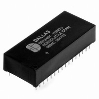
DS1245Y-100 Maxim Integrated Products, DS1245Y-100 Datasheet
DS1245Y-100
Specifications of DS1245Y-100
Available stocks


Related parts for DS1245Y-100


DS1245Y-100 Summary of contents
Page 1
... Low-power CMOS Read and write access times Lithium energy source is electrically disconnected to retain freshness until power is applied for the first time Full ±10% V operating range (DS1245Y) CC Optional ±5% V operating range CC (DS1245AB) Optional industrial temperature range of -40° ...
Page 2
... ODW DATA RETENTION MODE The DS1245AB provides full functional capability for V 4.5 volts. The DS1245Y provides full functional capability for V protects by 4.25 volts. Data is maintained in the absence of V The nonvolatile static RAMs constantly monitor V automatically write-protect themselves, all inputs become “don’t care,” and all outputs become high impedance ...
Page 3
... After a DS1245 PCM is reflow soldered, a DS9034PC PowerCap is snapped on top of the PCM to form a complete Nonvolatile SRAM module. The DS9034PC is keyed to prevent improper attachment. DS1245 PowerCap Modules and DS9034PC PowerCaps are ordered separately and shipped in separate containers. See the DS9034PC data sheet for further information DS1245Y/AB ...
Page 4
... See Note 10) A TYP MAX UNITS NOTES 5.0 5.25 V 5 ±5% for DS1245AB ±10% for DS1245Y) CC TYP MAX UNITS NOTES µA +1.0 µA +1 µA 200 600 µA 50 150 85 mA 4.62 4.75 V 4.37 4 ...
Page 5
... Output Hold from Address Change Write Cycle Time Write Pulse Width Address Setup Time Write Recovery Time Output High Z from WE Output Active from WE Data Setup Time Data Hold Time = 5V ±5% for DS1245AB ±10% for DS1245Y See Note 10 DS1245AB-70 DS1245Y-70 SYMBOL MIN MAX ...
Page 6
... READ CYCLE SEE NOTE 1 WRITE CYCLE 1 SEE NOTES and DS1245Y/AB ...
Page 7
... WRITE CYCLE 2 SEE NOTES and 13 POWER-DOWN/POWER-UP CONDITION DS1245Y/AB ...
Page 8
... REC SYMBOL MIN during write cycle, the output buffers remain in a high impedance state. IH and . t is measured from the latter going high going high DS1245Y/ See Note 10) A TYP MAX UNITS NOTES µs 1.5 µs µ 125 +25°C) A TYP MAX UNITS ...
Page 9
... Input pulse Rise and Fall Times SUPPLY TOLERANCE 5V ± ± ± ± ± 10% 5V ± 10% 5V ± 10% 5V ± 10% OUTLINE NO. MDT32+6 21-0245 PC2+3 21-0246 DS1245Y/AB SPEED GRADE PIN-PACKAGE (ns) 32 740 EDIP 70 34 PowerCap 740 EDIP 70 34 PowerCap 740 EDIP 70 34 PowerCap 740 EDIP ...
Page 10
... MIN/MAX information from the AC 11/10 Electrical Characteristics table; updated the Ordering Information table (removed -85, -100, and -120 parts and leaded -70 parts); removed the PowerCap module drawings and updated the Package Information table DESCRIPTION DS1245Y/AB PAGES CHANGED 10, 11 ...