DS1249Y-85IND Maxim Integrated Products, DS1249Y-85IND Datasheet
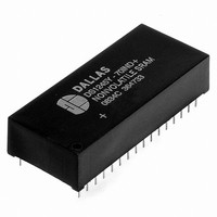
IC NVSRAM 2MBIT 85NS 32DIP

DS1249Y-85IND

Manufacturer Part Number
DS1249Y-85IND
Description
IC NVSRAM 2MBIT 85NS 32DIP
Manufacturer
Maxim Integrated Products
Datasheet

Specifications of DS1249Y-85IND

Format - Memory
RAM
Memory Type
NVSRAM (Non-Volatile SRAM)
Memory Size
2M (256K x 8)
Speed
85ns
Interface
Parallel
Voltage - Supply
4.5 V ~ 5.5 V
Operating Temperature
-40°C ~ 85°C
Package / Case
32-DIP Module (600 mil), 32-EDIP
Lead Free Status / RoHS Status
Contains lead / RoHS non-compliant

Available stocks

Company
Part Number
Manufacturer
Quantity
Price
Part Number:
DS1249Y-85IND
Manufacturer:
DALLAS
Quantity:
21
Part Number:
DS1249Y-85IND
Quantity:
29
Part Number:
DS1249Y-85IND#
Manufacturer:
Maxim Integrated Products
Quantity:
135
Part Number:
DS1249Y-85IND#
Manufacturer:
DALLAS
Quantity:
16
19-5631; Rev 11/10
FEATURES
 10 years minimum data retention in the
 Data is automatically protected during power
 Unlimited write cycles
 Low-power CMOS operation
 Read and write access times of 70 ns
 Lithium energy source is electrically
 Full ± 10% V
 Optional ± 5% V
 Optional industrial temperature range of
 JEDEC standard 32-pin DIP package
DESCRIPTION
The DS1249 2048k Nonvolatile SRAMs are 2,097,152-bit, fully static, nonvolatile SRAMs organized as
262,144 words by 8 bits. Each NV SRAM has a self-contained lithium energy source and control circuitry
which constantly monitors V
lithium energy source is automatically switched on and write protection is unconditionally enabled to
prevent data corruption. There is no limit on the number of write cycles which can be executed and no
additional support circuitry is required for microprocessor interfacing.
www.maxim-ic.com
absence of external power
loss
disconnected to retain freshness until power is
applied for the first time
(DS1249AB)
-40°C to +85°C, designated IND
CC
operating range (DS1249Y)
CC
operating range
CC
for an out-of-tolerance condition. When such a condition occurs, the
1 of 9
PIN ASSIGNMENT
PIN DESCRIPTION
A0 - A17
DQ0 - DQ7
V
GND
NC
CE
OE
WE
CC
2048k Nonvolatile SRAM
32-Pin ENCAPSULATED PACKAGE
GND
DQ0
DQ1
DQ2
A16
A14
A12
NC
A7
A6
A5
A4
A3
A2
A1
A0
740-mil EXTENDED
1
2
3
4
5
6
7
8
9
10
11
12
13
14
15
16
- Address Inputs
- Data In/Data Out
- Chip Enable
- Write Enable
- Output Enable
- Power (+5V)
- Ground
- No Connect
DS1249Y/AB
32
31
30
29
28
27
26
25
24
23
22
21
20
19
18
17
V
A15
A17
WE
A13
A8
A9
A11
OE
A10
CE
DQ7
DQ6
DQ5
DQ4
DQ3
CC

Related parts for DS1249Y-85IND

DS1249Y-85IND Summary of contents

Page 1

... Low-power CMOS operation  Read and write access times  Lithium energy source is electrically disconnected to retain freshness until power is applied for the first time  Full ± 10% V operating range (DS1249Y) CC  Optional ± operating range CC (DS1249AB)  Optional industrial temperature range of -40° ...

Page 2

... ODW DATA RETENTION MODE The DS1249AB provides full functional capability for V 4.5 volts. The DS1249Y provides full-functional capability for V protects by 4.25 volts. Data is maintained in the absence of V The nonvolatile static RAMs constantly monitor V automatically write protects themselves, all inputs become “don’t care,” and all outputs become high impedance ...

Page 3

... See Note 10) A TYP MAX UNITS NOTES 5.0 5.25 V 5 ±5% for DS1249AB ±10% for DS1249Y) CC TYP MAX UNITS NOTES µA +2.0 µA +2 1.0 1.5 mA µA 100 150 85 mA 4.62 4.75 V 4.37 4 ...

Page 4

... Write Recovery Time Output High-Z from WE Output Active from WE Data Setup Time Data Hold Time ( See Note 10 DS1249AB-70 DS1249Y-70 SYMBOL MIN ACC COE WR1 t 15 WR2 t ODW t 5 OEW DH1 t DH2 DS1249Y/ ±5% for DS1249AB ±10% for DS1249Y) UNITS NOTES MAX ...

Page 5

... READ CYCLE SEE NOTE 1 WRITE CYCLE 1 SEE NOTES and DS1249Y/AB ...

Page 6

... WRITE CYCLE 2 SEE NOTES and 13 POWER-DOWN/POWER-UP CONDITION SEE NOTE DS1249Y/AB ...

Page 7

... IH and . t is measured from the latter going high going high going high. WE going high DS1249Y/ See Note 10) A TYP MAX UNITS NOTES µs 1.5 µs µ 125 +25°C) A TYP MAX ...

Page 8

... Timing Measurement Reference Levels Input: 1.5V Output: 1.5V Input pulse Rise and Fall Times SUPPLY PIN-PACKAGE TOLERANCE 5V ± 740 EDIP 5V ± 740 EDIP 5V ± 10% 32 740 EDIP 5V ± 10% 32 740 EDIP OUTLINE NO. MDT32#7 21-0245 DS1249Y/AB SPEED GRADE (ns Note that a “+”, LAND PATTERN NO. — ...

Page 9

... Updated the storage information, soldering temperature, and lead temperature information in the Absolute Maximum Ratings section; 11/10 removed the -100 MIN/MAX information from the AC Electrical Characteristics table; updated the Ordering Information table (removed - 100 parts and leaded -70 parts); updated the Package Information table DESCRIPTION DS1249Y/AB PAGES CHANGED ...

Related keywords