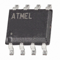
AT24C256N-10SC Atmel, AT24C256N-10SC Datasheet

AT24C256N-10SC
Specifications of AT24C256N-10SC
Available stocks
Related parts for AT24C256N-10SC
AT24C256N-10SC Summary of contents
Page 1
... Description The AT24C128/256 provides 131,072/262,144 bits of serial electrically erasable and programmable read only memory (EEPROM) organized as 16,384/32,768 words of 8 bits each. The device’s cascadable feature allows devices to share a common 2-wire bus. The device is optimized for use in many industrial and commercial applica- tions where low power and low voltage operation are essential ...
Page 2
... WRITE PROTECT (WP): The write protect input, when tied to GND, allows normal write operations. When WP is tied high all write operations to the memory are inhib- CC ited. If left unconnected internally pulled down to GND. Switching prior to a write operation cre- CC ates a software write protect function ...
Page 3
Pin Capacitance Applicable over recommended operating range from T Symbol Test Condition C Input/Output Capacitance (SDA) I/O C Input Capacitance (A IN Note: This parameter is characterized and is not 100% tested. DC Characteristics Applicable over recommended operating range ...
Page 4
... STOP bit and the completion of any internal operations. MEMORY RESET: After an interruption in protocol, power loss or system reset, any 2-wire part can be reset by follow- ing these steps: (a) Clock cycles, (b) look for SDA high in each cycle while SCL is high and then (c) create a start condition as SDA is high ...
Page 5
Bus Timing (SCL: Serial Clock, SDA: Serial Data I/O) Write Cycle Timing (SCL: Serial Clock, SDA: Serial Data I/O) SCL SDA 8th BIT WORD n Note: 1. The write cycle time t WR cycle. ACK STOP CONDITION is the time ...
Page 6
Data Validity Start and Stop Definition Output Acknowledge AT24C128/256 6 ...
Page 7
... This address stays valid between operations as long as the CC chip power is maintained. The address “roll over” during read is from the last byte of the last memory page, to the first byte of the first page. Once the device address with the read/write select bit set to one is clocked in and acknowledged by the EEPROM, the current address data word is serially clocked out ...
Page 8
Figure 1. Device Address Figure 2. Byte Write Figure 3. Page Write (* = DON’T CARE bit) († = DON’T CARE bit for the 128K) Figure 4. Current Address Read AT24C128/256 8 ...
Page 9
Figure 5. Random Read (* = DON’T CARE bit) († = DON’T CARE bit for the 128K) Figure 6. Sequential Read 9 ...
Page 10
AT24C128 Ordering Information t (max) I (max) I (max (ms 3000 6.0 3000 6.0 10 1500 0.5 1500 0.5 8C 8-Lead, 0.230" Wide, Leadless Array Package (LAP) 8C1 8-Lead, 0.300" Wide, Leadless ...
Page 11
AT24C128 Ordering Information (Continued) t (max) I (max (ms 800 800 8C 8-Lead, 0.230" Wide, Leadless Array Package (LAP) 8C1 8-Lead, 0.300" Wide, Leadless Array Package (LAP) 8P3 8-Lead, 0.300" Wide, ...
Page 12
... MAX (kHz) Ordering Code 1000 AT24C256-10PC AT24C256N-10SC AT24C256W-10SC AT24C256-10CC AT24C256C1-10CC AT24C256T1-10TC 1000 AT24C256-10PI AT24C256N-10SI AT24C256W-10SI AT24C256-10CI AT24C256C1-10CI AT24C256T1-10TI 400 AT24C256-10PC-2.7 AT24C256N-10SC-2.7 AT24C256W-10SC-2.7 AT24C256-10CC-2.7 AT24C256C1-10CC-2.7 AT24C256T1-10TC-2.7 400 AT24C256-10PI-2.7 AT24C256N-10SI-2.7 AT24C256W-10SI-2.7 AT24C256-10CI-2.7 AT24C256C1-10CI-2.7 AT24C256T1-10TI-2.7 Package Type Options Package Operation Range 8P3 Commercial 8S1 ...
Page 13
... Wide, Thin Shrink Small Outline Package (TSSOP) Blank Standard Operation (4.5V to 5.5V) -2.7 Low-Voltage (2.7V to 5.5V) -1.8 Low-Voltage (1.8V to 3.6V) (max) f MAX (kHz) Ordering Code 0.2 100 AT24C256-10PC-1.8 AT24C256N-10SC-1.8 AT24C256W-10SC-1.8 AT24C256-10CC-1.8 AT24C256C1-10CC-1.8 AT24C256T1-10TC-1.8 0.2 100 AT24C256-10PI-1.8 AT24C256N-10SI-1.8 AT24C256W-10SI-1.8 AT24C256-10CI-1.8 AT24C256C1-10CI-1.8 AT24C256T1-10TI-1.8 Package Type Options ...
Page 14
Packaging Information 8C, 8-Lead, 0.230" Wide, Leadless Array Package (LAP) Dimensions in Inches and (Millimeters) TOP VIEW 5.15 (0.203) 4.85 (0.191) 6.15 (0.242) 5.85 (0.230) BOTTOM VIEW 1.27 (0.050) TYP 0.64 (0.025) ...
Page 15
Packaging Information 8S2, 8-Lead, 0.200" Wide, Plastic Gull Wing Small Outline (EIAJ SOIC) Dimensions in Inches and (Millimeters) .020 (.508) .012 (.305) .213 (5.41) .205 (5.21) PIN 1 .050 (1.27) BSC .212 (5.38) .203 (5.16) .013 (.330) .004 (.102) 0 ...


