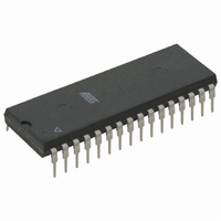
AT29C010A-12PC Atmel, AT29C010A-12PC Datasheet - Page 5

AT29C010A-12PC
Manufacturer Part Number
AT29C010A-12PC
Description
IC FLASH 1MBIT 120NS 32DIP
Manufacturer
Atmel
Datasheet
1.AT29C010A-70JU.pdf
(18 pages)
Specifications of AT29C010A-12PC
Format - Memory
FLASH
Memory Type
FLASH
Memory Size
1M (128K x 8)
Speed
120ns
Interface
Parallel
Voltage - Supply
4.5 V ~ 5.5 V
Operating Temperature
0°C ~ 70°C
Package / Case
32-DIP (0.600", 15.24mm)
Lead Free Status / RoHS Status
Contains lead / RoHS non-compliant
Other names
AT29C010A12PC
Available stocks
Company
Part Number
Manufacturer
Quantity
Price
Company:
Part Number:
AT29C010A-12PC
Manufacturer:
PANASONIC
Quantity:
4 000
Part Number:
AT29C010A-12PC
Manufacturer:
ATMEL/爱特梅尔
Quantity:
20 000
4.8
4.9
4.10
4.10.1
0394i–FLASH–9/08
Toggle Bit
Optional Chip Erase Mode
Boot Block Programming Lockout
Boot Block Lockout Detection
In addition to DATA polling the AT29C010A provides another method for determining the end of
a program or erase cycle. During a program or erase operation, successive attempts to read
data from the device will result in I/O6 toggling between one and zero. Once the program cycle
has completed, I/O6 will stop toggling and valid data will be read. Examining the toggle bit may
begin at any time during a program cycle.
The entire device can be erased by using a 6-byte software code. Please see Software Chip
Erase application note for details.
The AT29C010A has two designated memory blocks that have a programming lockout feature.
This feature prevents programming of data in the designated block once the feature has been
enabled. Each of these blocks consists of 8K bytes; the programming lockout feature can be set
independently for either block. While the lockout feature does not have to be activated, it can be
activated for either or both blocks.
These two 8K memory sections are referred to as boot blocks. Secure code which will bring up a
system can be contained in a boot block. The AT29C010A blocks are located in the first 8K
bytes of memory and the last 8K bytes of memory. The boot block programming lockout feature
can therefore support systems that boot from the lower addresses of memory or the higher
addresses. Once the programming lockout feature has been activated, the data in that block can
no longer be erased or programmed; data in other memory locations can still be changed
through the regular programming methods. To activate the lockout feature, a series of seven
program commands to specific addresses with specific data must be performed. Please see
Boot Block Lockout Feature Enable Algorithm.
If the boot block lockout feature has been activated on either block, the chip erase function will
be disabled.
A software method is available to determine whether programming of either boot block section is
locked out. See Software Product Identification Entry and Exit sections. When the device is in
the software product identification mode, a read from location 00002 will show if programming
the lower address boot block is locked out while reading location 1FFF2 will do so for the upper
boot block. If the data is FE, the corresponding block can be programmed; if the data is FF, the
program lockout feature has been activated and the corresponding block cannot be pro-
grammed. The software product identification exit mode should be used to return to standard
operation.
AT29C010A
5


