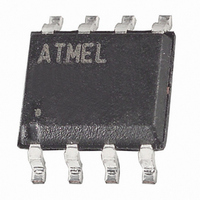
AT45DB011-SC Atmel, AT45DB011-SC Datasheet - Page 6

AT45DB011-SC
Manufacturer Part Number
AT45DB011-SC
Description
IC FLASH 1MBIT 13MHZ 8SOIC
Manufacturer
Atmel
Datasheet
1.AT45DB011-JC.pdf
(20 pages)
Specifications of AT45DB011-SC
Format - Memory
FLASH
Memory Type
DataFLASH
Memory Size
1M (512 pages x 264 bytes)
Speed
13MHz
Interface
SPI, 3-Wire Serial
Voltage - Supply
2.7 V ~ 3.6 V
Operating Temperature
0°C ~ 70°C
Package / Case
8-SOIC (5.3mm Width), 8-SOP, 8-SOEIAJ
Lead Free Status / RoHS Status
Contains lead / RoHS non-compliant
Other names
AT45DB011SC
Available stocks
Company
Part Number
Manufacturer
Quantity
Price
Company:
Part Number:
AT45DB011-SC
Manufacturer:
HARR
Quantity:
55
Part Number:
AT45DB011-SC
Manufacturer:
ATMEL/爱特梅尔
Quantity:
20 000
Buffer to Main Memory Page Program with Built-in Erase,
Buffer to Main Memory Page Program without Built-in
Erase, Page Erase, Block Erase, Main Memory Page Pro-
gram, and Auto Page Rewrite.
The result of the most recent Main Memory Page to Buffer
Compare operation is indicated using bit 6 of the status
register. If bit 6 is a 0, then the data in the main memory
page matches the data in the buffer. If bit 6 is a 1, then at
least one bit of the data in the main memory page does not
match the data in the buffer.
The device density is indicated using bits 5, 4, and 3 of the
status register. For the AT45DB011, the three bits are 0, 0,
and 1. The decimal value of these three binary bits does
not equate to the device density; the three bits represent a
combinational code relating to differing densities of Serial
DataFlash devices, allowing a total of eight different density
configurations.
HARDWARE PAGE WRITE PROTECT: If the WP pin is
held low, the first 256 pages of the main memory cannot be
reprogrammed. The only way to reprogram the first 256
pages is to first drive the protect pin high and then use the
program commands previously mentioned. The WP pin is
internally pulled high; therefore, in low pin count applica-
tions, connection of the WP pin is not necessary if this pin
and feature will not be utilized. However, it is recom-
mended that the WP pin be driven high externally
whenever possible.
RESET: A low state on the reset pin (RESET) will terminate
the operation in progress and reset the internal state
Status Register Format
Absolute Maximum Ratings*
DC and AC Operating Range
Note:
6
Temperature under Bias ................................ -55°C to +125°C
Storage Temperature ..................................... -65°C to +150°C
All Input Voltages
(including NC Pins)
with Respect to Ground ...................................-0.6V to +6.25V
All Output Voltages
with Respect to Ground .............................-0.6V to V
Operating Temperature (Case)
V
CC
RDY/BUSY
Power Supply
Bit 7
1. After power is applied and V
tional mode is started.
(1)
AT45DB011
COMP
Bit 6
Com.
Ind.
CC
is at the minimum specified datasheet value, the system should wait 20 ms before an opera-
Bit 5
0
CC
+ 0.6V
Bit 4
0
machine to an idle state. The device will remain in the reset
condition as long as a low level is present on the RESET
pin. Normal operation can resume once the RESET pin is
brought back to a high level.
The device incorporates an internal power-on reset circuit,
so there are no restrictions on the RESET pin during
power-on sequences. The RESET pin is also internally
pulled high; therefore, in low pin count applications, con-
nection of the RESET pin is not necessary if this pin and
feature will not be utilized. However, it is recommended
that the RESET pin be driven high externally whenever
possible.
READY/BUSY: This open drain output pin will be driven
low when the device is busy in an internally self-timed oper-
ation. This pin, which is normally in a high state (through an
external pull-up resistor), will be pulled low during program-
ming operations, compare operations, and during page-to-
buffer transfers.
The busy status indicates that the Flash memory array and
the buffer cannot be accessed.
Power-on/Reset State
When power is first applied to the device, or when recover-
ing from a reset condition, the device will default to SPI
Mode 3. In addition, the SO pin will be in a high-impedance
state, and a high-to-low transition on the CS pin will be
required to start a valid instruction. The SPI mode will be
automatically selected on every falling edge of CS by sam-
pling the inactive clock state.
*NOTICE:
Bit 3
1
-40 ° C to 85 ° C
AT45DB011
Stresses beyond those listed under “Absolute
Maximum Ratings” may cause permanent dam-
age to the device. This is a stress rating only and
functional operation of the device at these or any
other conditions beyond those indicated in the
operational sections of this specification is not
implied. Exposure to absolute maximum rating
conditions for extended periods may affect device
reliability.
2.7V to 3.6V
0 ° C to 70 ° C
Bit 2
X
Bit 1
X
Bit 0
X


