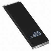
AT49BV002-12TC Atmel, AT49BV002-12TC Datasheet - Page 6

AT49BV002-12TC
Manufacturer Part Number
AT49BV002-12TC
Description
IC FLASH 2MBIT 120NS 32TSOP
Manufacturer
Atmel
Datasheet
1.AT49BV002-90JC.pdf
(26 pages)
Specifications of AT49BV002-12TC
Format - Memory
FLASH
Memory Type
FLASH
Memory Size
2M (256K x 8)
Speed
120ns
Interface
Parallel
Voltage - Supply
2.7 V ~ 3.6 V
Operating Temperature
0°C ~ 70°C
Package / Case
32-TSOP
Lead Free Status / RoHS Status
Contains lead / RoHS non-compliant
Other names
AT49BV00212TC
Command Definition (in Hex)
Notes:
Absolute Maximum Ratings
6
Command
Sequence
Read
Chip Erase
Sector Erase
Byte Program
Boot Block Lockout
Product ID Entry
Product ID Exit
Product ID Exit
Temperature Under Bias................................ -55°C to +125°C
Storage Temperature ..................................... -65°C to +150°C
All Input Voltages
(including NC Pins)
with Respect to Ground ...................................-0.6V to +6.25V
All Output Voltages
with Respect to Ground .............................-0.6V to V
Voltage on OE
with Respect to Ground ...................................-0.6V to +13.5V
1. The DATA FORMAT in each bus cycle is as follows: I/O7 - I/O0 (Hex)
2. The 16K byte boot sector has the address range 00000H to 03FFFH for the AT49BV/LV002(N) and 3C000H to 3FFFFH for
3. Either one of the Product ID Exit commands can be used.
4. SA = sector addresses:
AT49BV/LV002(N)(T)
the AT49BV/LV002(N)T
For the AT49BV/LV002(N):
SA = 00000 to 03FFF for BOOT BLOCK
Nothing will happen and the device goes back to the read mode in 100 ns
SA = 04000 to 05FFF for PARAMETER BLOCK 1
SA = 06000 to 07FFF for PARAMETER BLOCK 2
SA = 08000 to 1FFFF for MAIN MEMORY ARRAY BLOCK 1
This command will erase - PB1, PB2 and MMB1
SA = 20000 to 3FFFF for MAIN MEMORY ARRAY BLOCK 2
For the AT49BV/LV002(N)T:
SA = 3C000 to 3FFFF for BOOT BLOCK
Nothing will happen and the device goes back to the read mode in 100 ns
SA = 3A000 to 3BFFF for PARAMETER BLOCK 1
SA = 38000 to 39FFF for PARAMETER BLOCK 2
SA = 20000 to 37FFF for MAIN MEMORY ARRAY BLOCK 1
This command will erase - PB1, PB2 and MMB1
SA = 00000 to IFFFF for MAIN MEMORY ARRAY BLOCK 2
(3)
(3)
(2)
Cycles
Bus
1
6
6
4
6
3
3
1
XXXX
Addr
5555
5555
5555
5555
5555
5555
Addr
1st Bus
Cycle
Data
D
AA
AA
AA
AA
AA
AA
F0
OUT
(1)
CC
2AAA
2AAA
2AAA
2AAA
2AAA
2AAA
Addr
2nd Bus
+ 0.6V
Cycle
Data
55
55
55
55
55
55
*NOTICE:
Addr
5555
5555
5555
5555
5555
5555
3rd Bus
Cycle
Data
A0
F0
Stresses beyond those listed under “Absolute Maxi-
mum Ratings” may cause permanent damage to the
device. This is a stress rating only and functional
operation of the device at these or any other condi-
tions beyond those indicated in the operational sec-
tions of this specification is not implied. Exposure to
absolute maximum rating conditions for extended
periods may affect device reliability.
80
80
80
90
Addr
5555
5555
5555
Addr
4th Bus
Cycle
Data
AA
D
AA
AA
IN
2AAA
2AAA
2AAA
Addr
5th Bus
Cycle
Data
55
55
55
0982D–FLASH–02/03
Addr
5555
SA
5555
6th Bus
(4)
Cycle
Data
10
30
40


