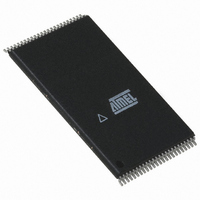
AT49BV8192AT-12TC Atmel, AT49BV8192AT-12TC Datasheet - Page 7

AT49BV8192AT-12TC
Manufacturer Part Number
AT49BV8192AT-12TC
Description
IC FLASH 8MBIT 120NS 48TSOP
Manufacturer
Atmel
Datasheet
1.AT49BV8192A-11CI.pdf
(20 pages)
Specifications of AT49BV8192AT-12TC
Format - Memory
FLASH
Memory Type
FLASH
Memory Size
8M (1M x 8 or 512K x 16)
Speed
120ns
Interface
Parallel
Voltage - Supply
2.7 V ~ 3.6 V
Operating Temperature
0°C ~ 70°C
Package / Case
48-TSOP
Lead Free Status / RoHS Status
Contains lead / RoHS non-compliant
Other names
AT49BV8192AT12TC
Available stocks
Company
Part Number
Manufacturer
Quantity
Price
Part Number:
AT49BV8192AT-12TC
Manufacturer:
ATMEL/爱特梅尔
Quantity:
20 000
Command Definition in Hex
Notes:
Absolute Maximum Ratings*
1049K–FLASH–11/02
Command
Sequence
Read
Chip Erase
Sector Erase
Byte/Word Program
Boot Block Lockout
Product ID Entry
Product ID Exit
Product ID Exit
Temperature under Bias ................................ -55°C to +125°C
Storage Temperature ..................................... -65°C to +150°C
All Input Voltages
(including NC Pins)
with Respect to Ground ...................................-0.6V to +6.25V
All Output Voltages
with Respect to Ground .............................-0.6V to V
Voltage on RESET
with Respect to Ground ...................................-0.6V to +13.5V
1. The DATA FORMAT in each bus cycle is as follows: I/O15 - I/O8 (Don’t Care); I/O7 - I/O0 (Hex)
2. The boot sector has the address range
3. Either one of the Product ID Exit commands can be used.
4. SA = sector addresses: (A0 - A18)
The ADDRESS FORMAT in each bus cycle is as follows: A15 - A0 (Hex), A-1, and A15 - A18 (Don’t Care)
AT49BV/LV008AT; 00000H to 01FFFH for the AT49BV/LV8192A; and 7E000H to 7FFFFH for the
AT49BV/LV8192AT
For the AT49BV/LV008A/8192A
SA = 01XXX for BOOT BLOCK
SA = 02XXX for PARAMETER BLOCK 1
SA = 03XXX for PARAMETER BLOCK 2
SA = 7FXXX for MAIN MEMORY ARRAY
For the AT49BV/LV008AT/8192AT
SA = 7FXXX for BOOT BLOCK
SA = 7DXXX for PARAMETER BLOCK 1
SA = 7CXXX for PARAMETER BLOCK 2
SA = 7BXXX for MAIN MEMORY ARRAY
(3)
(3)
(2)
Cycles
Bus
1
6
6
4
6
3
3
1
.
Addr
5555
5555
5555
5555
5555
5555
Addr
xxxx
1st Bus
Cycle
D
Data
(1)
AA
AA
AA
AA
AA
AA
F0
OUT
00000H to 03FFFH for the AT49BV/LV008A; FC000H to FFFFFH for the
2AAA
2AAA
2AAA
2AAA
2AAA
2AAA
Addr
CC
2nd Bus
+ 0.6V
Cycle
Data
55
55
55
55
55
55
Addr
5555
5555
5555
5555
5555
5555
*NOTICE:
3rd Bus
Cycle
AT49BV/LV008A(T)/8192A(T)
Data
80
80
A0
80
90
F0
Stresses beyond those listed under “Absolute
Maximum Ratings” may cause permanent dam-
age to the device. This is a stress rating only and
functional operation of the device at these or any
other conditions beyond those indicated in the
operational sections of this specification is not
implied. Exposure to absolute maximum rating
conditions for extended periods may affect
device reliability.
Addr
5555
5555
5555
Addr
4th Bus
Cycle
Data
AA
AA
D
AA
IN
2AAA
2AAA
2AAA
Addr
5th Bus
Cycle
Data
55
55
55
Addr
5555
SA
5555
6th Bus
(4)
Cycle
Data
10
30
40
7


