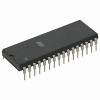
AT49F002-12PI Atmel, AT49F002-12PI Datasheet

AT49F002-12PI
Specifications of AT49F002-12PI
Related parts for AT49F002-12PI
AT49F002-12PI Summary of contents
Page 1
... Typical 10,000 Write Cycles Description The AT49F002(N)( 5-volt only in-system reprogrammable Flash memory. Its 2 megabits of memory is organized as 262,144 words by 8 bits. Manufactured with Atmel’s advanced nonvolatile CMOS technology, the device offers access times with power dissipation of just 275 mW over the commercial temperature range. ...
Page 2
... When the device is deselected, the CMOS standby current is less than 100 µA. For the AT49F002N(T) pin 1 for the DIP and PLCC packages and pin 9 for the TSOP package are don’t connect pins. To allow for simple in-system reprogrammability, the AT49F002(N)(T) does not require high input voltages for programming ...
Page 3
... This feature does not have to be acti- vated; the boot block’s usage as a write protected region is optional to the user. The address range of the boot block is 00000 to 03FFF for the AT49F002(N) while the address AT49F002(N)(T) cycle BP ...
Page 4
... AT49F002(N), and a read from address location 3C002H will show if programming the boot block is locked out for AT49F002(N)T. If the data on I/O0 is low, the boot block can be programmed; if the data on I/O0 is high, the program lockout feature has been activated and the block cannot be programmed ...
Page 5
... XXXX Notes: 1. The DATA FORMAT in each bus cycle is as follows: I/O7 - I/O0 (Hex) 2. The 16K byte boot sector has the address range 00000H to 03FFFH for the AT49F002(N) and 3C000H to 3FFFFH for the AT49F002(N)T 3. Either one of the Product ID Exit commands can be used. ...
Page 6
... Notes can IH. 2. Refer to AC Programming Waveforms 12.0V 0.5V Manufacturer Code: 1FH, Device Code: 07H - AT49F002(N), 08H - AT49F002(N)T 5. See details under Software Product Identification Entry/Exit. 6. This pin is not available on the AT49F002N(T). DC Characteristics Symbol Parameter I Input Load Current LI I Output Leakage Current ...
Page 7
... ADDRESS ADDRESS VALID ACC HIGH Z OUTPUT OUTPUT - t after the address transition without impact on t ACC after the falling edge of CE without impact Output Load Test Max 6 12 AT49F002(N)(T) -90 -12 Min Max Min VALID . ACC after an address change CE ACC 70/90/120 ns 5.0V 5.0V 1 ...
Page 8
... Chip Select Set-up Time CS t Chip Select Hold Time CH t Write Pulse Width ( Data Set-up Time Data, OE Hold Time DH OEH t Write Pulse Width High WPH AC Byte Load Waveforms WE Controlled OE ADDRESS CE WE DATA IN CE Controlled OE ADDRESS WE CE DATA IN AT49F002(N)( OES OES Min Max 0 50 ...
Page 9
... OE must be high only when WE and CE are both low. 2. For chip erase, the address should be 5555. For sector erase, the address depends on what sector erased. (See note 4 under command definitions.) 3. For chip erase, the data should be 10H, and for sector erase, the data should be 30H. AT49F002(N)(T) Min Typ Max ...
Page 10
... OE (1)(2)(3) Toggle Bit Waveforms I/O6 Notes: 1. Toggling either both OE and CE will operate toggle bit. The t input(s). 2. Beginning and ending state of I/O6 will vary. 3. Any address location may be used but the address should not vary. AT49F002(N)(T) 10 (1) t OEH t OE HIGH (1) ...
Page 11
... IL Manufacture Code is read for Device Code is read for The device does not remain in identification mode if powered down. 4. The device returns to standard operation mode. 5. Manufacturer Code: 1FH Device Code: 07H - AT49F002(N) 08H - AT49F002(N)T (1) Boot Block Lockout Feature Enable Algorithm (1) LOAD DATA F0 TO ...
Page 12
... AT49F002-90TC 32T AT49F002-90VC 32V AT49F002-90JI 32J AT49F002-90PI 32P6 AT49F002-90TI 32T AT49F002-90VI 32V AT49F002-12JC 32J AT49F002-12PC 32P6 AT49F002-12TC 32T AT49F002-12VC 32V AT49F002-12JI 32J AT49F002-12PI 32P6 AT49F002-12TI 32T AT49F002-12VI 32V Package Type Operation Range Commercial ( Industrial (- Commercial ( Industrial (- Commercial ( Industrial (- Commercial ( Industrial ...
Page 13
... AT49F002N Ordering Information I (mA ACC (ns) Active Standby 55 50 0 0 0.1 50 0.3 120 50 0.1 50 0.3 32J 32-lead, Plastic J-leaded Chip Carrier Package (PLCC) 32P6 32-pin, 0.600" Wide, Plastic Dual Inline Package (PDIP) 32T 32-lead, Plastic Thin Small Outline Package (TSOP mm) ...
Page 14
... AT49F002T Ordering Information I (mA ACC (ns) Active Standby 55 50 0 0 0.1 50 0.3 120 50 0.1 50 0.3 32J 32-lead, Plastic J-leaded Chip Carrier Package (PLCC) 32P6 32-pin, 0.600" Wide, Plastic Dual Inline Package (PDIP) 32T 32-lead, Plastic Thin Small Outline Package (TSOP mm) ...
Page 15
... AT49F002NT Ordering Information I (mA ACC (ns) Active Standby 55 50 0 0 0.1 50 0.3 120 50 0.1 50 0.3 32J 32-lead, Plastic J-leaded Chip Carrier Package (PLCC) 32P6 32-pin, 0.600" Wide, Plastic Dual Inline Package (PDIP) 32T 32-lead, Plastic Thin Small Outline Package (TSOP mm) ...
Page 16
... REF 0.70(.028) 0.50(.020) *Controlling dimension: millimeters AT49F002(N)(T) 16 32P6, 32-pin, 0.600" Wide, Plastic Dual Inline Package (PDIP) Dimensions in Inches and (Millimeters) .025(.635) X 30˚ - 45˚ .012(.305) .008(.203) .530(13.5) ...
Page 17
... No licenses to patents or other intellectual prop- erty of Atmel are granted by the Company in connection with the sale of Atmel products, expressly or by implication. Atmel’s products are not authorized for use as critical components in life suppor t devices or systems. ...


