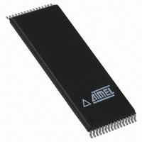
AT49LV040-12TC Atmel, AT49LV040-12TC Datasheet

AT49LV040-12TC
Specifications of AT49LV040-12TC
Related parts for AT49LV040-12TC
AT49LV040-12TC Summary of contents
Page 1
... I/O3 A18 9 24 GND A16 10 23 I/O2 A15 11 22 I/O1 A12 4-megabit (512K x 8) Single 2.7-volt ™ Battery-Voltage Flash Memory AT49BV040 AT49LV040 Not Recommended for New Design Contact Atmel to discuss the latest design in trends and options Rev. 0679D–03/01 1 ...
Page 2
... ERASURE: Before a byte can be reprogrammed, the 512K bytes memory array (or 496K bytes if the boot block fea- tured is used) must be erased. The erased state of the memory bits is a logical “1”. The entire device can be erased at one time by using a six-byte software code ...
Page 3
... The software product identification code should be used to return to standard operation. PRODUCT IDENTIFICATION: The product identification mode identifies the device and manufacturer as Atmel. It may be accessed by hardware or software operation. The hardware operation mode can be used by an external pro- grammer to identify the correct programming algorithm for the Atmel product. For details, see “ ...
Page 4
Command Definition (in Hex) Command Bus Sequence Cycles Addr Read 1 Addr Chip Erase 6 5555 Byte Program 4 5555 (1) Boot Block Lockout 6 5555 Product ID Entry 3 5555 (2) Product ID Exit 3 5555 (2) Product ID ...
Page 5
... Input Low Voltage IL V Input High Voltage IH V Output Low Voltage OL V Output High Voltage OH Notes the erase mode mA See details under “Software Product Identification Entry/Exit” on page 10. AT49LV040-70 AT49BV/LV040-90 0°C - 70°C -40°C - 85°C -40°C - 85°C 3.0V to 3.6V 2.7V to 3.6V/3. ...
Page 6
... Measurement Level < Pin Capacitance ( MHz 25°C Symbol Typ OUT Note: 1. This parameter is characterized and is not 100% tested. AT49BV/LV040 6 AT49LV040-70 Min Max after the address transition without impact on t ACC after the falling edge of CE without impact Output Test Load Max 6 12 ...
Page 7
AC Byte Load Characteristics Symbol Parameter Address, OE Setup Time AS OES t Address Hold Time AH t Chip Select Setup Time CS t Chip Select Hold Time CH t Write Pulse Width (WE or CE) WP ...
Page 8
Program Cycle Characteristics Symbol Parameter t Byte Programming Time BP t Address Setup Time AS t Address Hold Time AH t Data Setup Time DS t Data Hold Time DH t Write Pulse Width WP t Write Pulse Width High ...
Page 9
Data Polling Characteristics Symbol Parameter t Data Hold Time Hold Time OEH ( Output Delay OE t Write Recovery Time WR Notes: 1. These parameters are characterized and not 100% tested. 2. See t ...
Page 10
Software Product Identification Entry LOAD DATA AA TO ADDRESS 5555 LOAD DATA 55 TO ADDRESS 2AAA LOAD DATA 90 TO ADDRESS 5555 ENTER PRODUCT IDENTIFICATION (2)(3)(4) MODE Software Product Identification Exit OR LOAD DATA AA TO ADDRESS 5555 LOAD DATA ...
Page 11
... AT49BV040-90JI AT49BV040-90TI AT49BV040-90VI AT49BV040-12JC AT49BV040-12TC AT49BV040-12VC AT49BV040-12JI AT49BV040-12TI AT49BV040-12VI AT49LV040-70JC AT49LV040-70TC AT49LV040-70VC AT49LV040-70JI AT49LV040-70TI AT49LV040-70VI AT49LV040-90JC AT49LV040-90TC AT49LV040-90VC AT49LV040-90JI AT49LV040-90TI AT49LV040-90VI Package Type AT49BV/LV040 Package Operation Range 32J Commercial 32T (0°C to 70°C) 32V 32J Industrial 32T (-40°C to 85°C) 32V ...
Page 12
Packaging Information 32J, 32-lead, Plastic J-leaded Chip Carrier (PLCC) Dimensions in Inches and (Millimeters) JEDEC STANDARD MS-016 AE .045(1.14) X 45˚ PIN NO. 1 IDENTIFY .553(14.0) .547(13.9) .032(.813) .595(15.1) .026(.660) .585(14.9) .050(1.27) TYP .300(7.62) REF .430(10.9) .390(9.90) AT CONTACT POINTS ...
Page 13
... No licenses to patents or other intellectual property of Atmel are granted by the Company in connection with the sale of Atmel products, expressly or by implication. Atmel’s products are not authorized for use as critical components in life support devices or systems. ...


