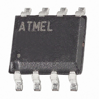
AT93C56-10SC-2.5 Atmel, AT93C56-10SC-2.5 Datasheet - Page 6

AT93C56-10SC-2.5
Manufacturer Part Number
AT93C56-10SC-2.5
Description
IC EEPROM 2KBIT 2MHZ 8SOIC
Manufacturer
Atmel
Datasheet
1.AT93C46-10PC.pdf
(16 pages)
Specifications of AT93C56-10SC-2.5
Format - Memory
EEPROMs - Serial
Memory Type
EEPROM
Memory Size
2K (256 x 8 or 128 x 16)
Speed
500kHz, 1MHz, 2MHz
Interface
3-Wire Serial
Voltage - Supply
2.5 V ~ 5.5 V
Operating Temperature
0°C ~ 70°C
Package / Case
8-SOIC (3.9mm Width)
Lead Free Status / RoHS Status
Contains lead / RoHS non-compliant
Other names
AT93C5610SC2.5
Available stocks
Company
Part Number
Manufacturer
Quantity
Price
Company:
Part Number:
AT93C56-10SC-2.5
Manufacturer:
ATMEL
Quantity:
4 890
Part Number:
AT93C56-10SC-2.5
Manufacturer:
ATMEL/爱特梅尔
Quantity:
20 000
Instruction Set for the AT93C56 and AT93C66
Functional Description
The AT93C46/56/57/66 is accessed via a simple and ver-
satile 3-wire serial communication interface. Device opera-
tion is controlled by seven instructions issued by the host
processor. A valid instruction starts with a rising edge
of CS and consists of a Start Bit (logic “1”) followed by the
appropriate Op Code and the desired memory Address
location.
READ (READ): The Read (READ) instruction contains
the Address code for the memory location to be read. After
the instruction and address are decoded, data from the
selected memory location is available at the serial output
pin DO. Output data changes are synchronized with the ris-
ing edges of serial clock SK. It should be noted that a
dummy bit (logic “0”) precedes the 8- or 16-bit data output
string.
ERASE/WRITE (EWEN): To assure data integrity, the
part automatically goes into the Erase/Write Disable
(EWDS) state when power is first applied. An Erase/Write
Enable (EWEN) instruction must be executed first before
any programming instructions can be carried out. Please
note that once in the Erase/Write Enable state, program-
ming remains enabled until an Erase/Write Disable
(EWDS) instruction is executed or V
from the part.
ERASE (ERASE): The Erase (ERASE) instruction pro-
grams all bits in the specified memory location to the logical
“1” state. The self-timed erase cycle starts once the
ERASE instruction and address are decoded. The DO pin
outputs the READY/BUSY status of the part if CS is
brought high after being kept low for a minimum of 250 ns
(t
ory location has been erased, and the part is ready for
another instruction.
6
Instruction
READ
EWEN
ERASE
WRITE
ERAL
WRAL
EWDS
CS
). A logic “1” at pin DO indicates that the selected mem-
AT93C46/56/57/66
SB
1
1
1
1
1
1
1
Code
Op
10
00
11
01
00
00
00
11XXXXXXX
10XXXXXXX
01XXXXXXX
00XXXXXXX
A
A
A
CC
8
8
8
x 8
- A
- A
- A
power is removed
0
0
0
Address
11XXXXXX
10XXXXXX
01XXXXXX
00XXXXXX
A
A
A
x 16
7
7
7 -
- A
- A
A
0
0
0
WRITE (WRITE): The Write (WRITE) instruction contains
the 8 or 16 bits of data to be written into the specified mem-
ory location. The self-timed programming cycle, t
after the last bit of data is received at serial data input pin
DI. The DO pin outputs the READY/BUSY status of the part
if CS is brought high after being kept low for a minimum of
250 ns (t
is still in progress. A logic “1” indicates that the memory
location at the specified address has been written with the
data pattern contained in the instruction and the part is
ready for further instructions. A READY/BUSY status can-
not be obtained if the CS is brought high after the end
of the self-timed programming cycle, t
ERASE ALL (ERAL): The Erase All (ERAL) instruction
programs every bit in the memory array to the logic “1”
state and is primarily used for testing purposes. The DO pin
outputs the READY/BUSY status of the part if CS is
brought high after being kept low for a minimum of 250 ns
(t
10%.
WRITE ALL (WRAL): The Write All (WRAL) instruction
programs all memory locations with the data patterns spec-
i f i e d i n t h e i n s t r u c t i o n . T h e D O p i n o u t p u t s t h e
READY/BUSY status of the part if CS is brought high after
being kept low for a minimum of 250 ns (t
instruction is valid only at V
ERASE/WRITE DISABLE (EWDS): To protect against
accidental data disturb, the Erase/Write Disable (EWDS)
instruction disables all programming modes and should be
executed after all programming operations. The operation
of the READ instruction is independent of both the EWEN
and EWDS instructions and can be executed at any time.
CS
D
D
7
7
x 8
). The ERAL instruction is valid only at V
- D
- D
0
0
Data
CS
). A logic “0” at DO indicates that programming
D
D
x 16
15
15
- D
- D
0
0
Comments
Reads data stored in memory, at
specified address.
programming modes.
Erases memory location A
Writes memory location A
only at V
Writes all memory locations. Valid
when V
Register cleared.
Write enable must precede all
Erases all memory locations. Valid
Disables all programming instructions.
CC
= 5.0V ± 10%.
CC
CC
= 5.0V ± 10% and Disable
= 4.5V to 5.5V.
WP
CS
.
). The WRAL
n
CC
n
- A
- A
WP
= 5.0V ±
0
0
.
.
, starts


