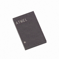
AT24C1024C1-10CI-2.7 Atmel, AT24C1024C1-10CI-2.7 Datasheet

AT24C1024C1-10CI-2.7
Specifications of AT24C1024C1-10CI-2.7
Available stocks
Related parts for AT24C1024C1-10CI-2.7
AT24C1024C1-10CI-2.7 Summary of contents
Page 1
... Description The AT24C1024 provides 1,048,576 bits of serial electrically erasable and program- mable read only memory (EEPROM) organized as 131,072 words of 8 bits each. The device’s cascadable feature allows up to two devices to share a common two-wire bus. The device is optimized for use in many industrial and commercial applications where low-power and low-voltage operation are essential ...
Page 2
Absolute Maximum Ratings* Operating Temperature..................................–55°C to +125°C Storage Temperature .....................................–65°C to +150°C Voltage on Any Pin with Respect to Ground .................................... –1.0V to +7.0V Maximum Operating Voltage .......................................... 6.25V DC Output Current........................................................ 5.0 mA Figure 1. Block Diagram AT24C1024 2 ...
Page 3
... AT24C1024, 1024K SERIAL EEPROM: The 1024K is internally organized as 512 pages of 256 bytes each. Random word addressing requires a 17-bit data word address. Organization 1471O–SEEPR–3/07 plane is <3 pF. If coupling is >3 pF, Atmel recommends connecting the A1 pin all write operations to the memory are CC plane is < ...
Page 4
Table 2. Pin Capacitance Applicable over recommended operating range from T Symbol Test Condition C Input/Output Capacitance (SDA) I/O C Input Capacitance (A , SCL Note: 1. This parameter is characterized and is not 100% tested. Table ...
Page 5
Table 4. AC Characteristics (1) Applicable over recommended operating range from T otherwise noted) Symbol Parameter f Clock Frequency, SCL SCL t Clock Pulse Width Low LOW t Clock Pulse Width High HIGH t Clock Low to Data Out Valid ...
Page 6
... STANDBY MODE: The AT24C1024 features a low-power standby mode which is enabled: a) upon power-up and b) after the receipt of the stop bit and the completion of any internal operations. MEMORY RESET: After an interruption in protocol, power loss or system reset, any two-wire part can be reset by following these steps: 1. Clock cycles. ...
Page 7
Figure 2. Bus Timing (SCL: Serial Clock, SDA: Serial Data I/O Figure 3. Write Cycle Timing (SCL: Serial Clock, SDA: Serial Data I/O) SCL SDA 8th BIT WORDn Note: 1. The write cycle time t is the time from a ...
Page 8
... DATA SECURITY: The AT24C1024 has a hardware data protection scheme that allows the user to write-protect the entire memory when the WP pin AT24C1024 the device address is a memory page address bit. This memory page 1471O–SEEPR–3/07 ...
Page 9
... Write BYTE WRITE: To select a data word in the 1024K memory requires a 17-bit word address. The word address field consists of the P Operations word address followed by the least significant word address (see Figure 8 on page 11) A write operation requires the P address word and acknowledgment. Upon receipt of this address, the EEPROM will again respond with a zero and then clock in the first 8-bit data word ...
Page 10
... The address “rollover” during read is from the last byte of the last memory page, to the first byte of the first page. Once the device address with the read/write select bit set to one is clocked in and acknowl- edged by the EEPROM, the current address data word is serially clocked out ...
Page 11
Figure 7. Device Address Figure 8. Byte Write Figure 9. Page Write P 0 Figure 10. Current Address Read 1471O–SEEPR–3/07 0 MOST LEAST SIGNIFICANT SIGNIFICANT P 0 MOST LEAST SIGNIFICANT SIGNIFICANT 11 ...
Page 12
Figure 11. Random Read P 0 Figure 12. Sequential Read High Byte ADDRESS P 0 AT24C1024 12 High Byte Low Byte ADDRESS ADDRESS Low Byte ADDRESS Data Data Data 1471O–SEEPR–3/07 ...
Page 13
... Ordering Information Ordering Code (2) AT24C1024C1-10CU-2.7 (2) AT24C1024-10PU-2.7 (2) AT24C1024W-10SU-2.7 (2) AT24C1024Y4-10YU-2.7 (3) AT24C1024-W2.7-11 Notes: 1. This device is not recommended for new design. Please refer to AT24C1024B datasheet. For 2.7V devices used in the 4.5V to 5.5V range, please refer to performance values in the AC and DC Characteristics tables. 2. “U” designates Green Package & RoHS compliant. ...
Page 14
Packaging Information 8CN1 – LAP Marked Pin1 Indentifier E 0.10 mm TYP Bottom View Note: 1. Metal Pad Dimensions. 2325 Orchard Parkway San Jose, CA 95131 R AT24C1024 14 D Top View Pin1 Corner ...
Page 15
PDIP Top View PLCS Side View Notes: 1. This drawing is for general information only; refer to JEDEC Drawing MS-001, Variation BA, for additional information. 2. Dimensions A and L are measured with the ...
Page 16
EIAJ SOIC 1 N Top View e D Side View Notes: 1. This drawing is for general information only; refer to EIAJ Drawing EDR-7320 for additional information. 2. Mismatch of the upper and lower dies and resin burrs ...
Page 17
SAP PIN 1 INDEX AREA D E 1150 E. Cheyenne Mtn. Blvd. Colorado Springs, CO 80906 R 1471O–SEEPR–3/07 A PIN COMMON DIMENSIONS (Unit of Measure = mm) SYMBOL MIN A – A1 0.00 ...
Page 18
Revision History Doc. Rev. 1471O AT24C1024 18 Date Comments 3/2007 Implemented revision history. Added ‘Not recommended for new design; please refer to AT24C1024B datasheet’ note to page 1 and page 13. 1471O–SEEPR–3/07 ...
Page 19
... Disclaimer: The information in this document is provided in connection with Atmel products. No license, express or implied, by estoppel or otherwise, to any intellectual property right is granted by this document or in connection with the sale of Atmel products. EXCEPT AS SET FORTH IN ATMEL’S TERMS AND CONDI- TIONS OF SALE LOCATED ON ATMEL’S WEB SITE, ATMEL ASSUMES NO LIABILITY WHATSOEVER AND DISCLAIMS ANY EXPRESS, IMPLIED OR STATUTORY WARRANTY RELATING TO ITS PRODUCTS INCLUDING, BUT NOT LIMITED TO, THE IMPLIED WARRANTY OF MERCHANTABILITY, FITNESS FOR A PARTICULAR PURPOSE, OR NON-INFRINGEMENT ...


