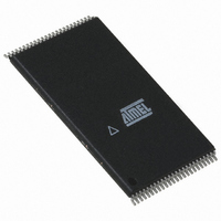
AT49BV161-90TI Atmel, AT49BV161-90TI Datasheet - Page 3

AT49BV161-90TI
Manufacturer Part Number
AT49BV161-90TI
Description
IC FLASH 16MBIT 90NS 48TSOP
Manufacturer
Atmel
Datasheet
1.AT49BV160-70CI.pdf
(29 pages)
Specifications of AT49BV161-90TI
Format - Memory
FLASH
Memory Type
FLASH
Memory Size
16M (2M x 8 or 1M x 16)
Speed
90ns
Interface
Parallel
Voltage - Supply
2.65 V ~ 3.3 V
Operating Temperature
-40°C ~ 85°C
Package / Case
48-TSOP
Lead Free Status / RoHS Status
Contains lead / RoHS non-compliant
AT49BV/LV160(T)/161(T)
The device powers on in the read mode. Command sequences are used to place the device in
other operation modes such as program and erase. The device has the capability to protect
the data in any sector. (See “Sector Lockdown” section.)
To increase the flexibility of the device, it contains an Erase Suspend and Program Suspend
feature. This feature will put the Erase or Program on hold for any amount of time and let the
user read data from or program data to any of the remaining sectors within the memory. The
end of a program or an erase cycle is detected by the Ready/Busy pin, Data Polling or by the
toggle bit.
The VPP pin provides data protection and faster programming. When the V
input is below
PP
0.8V, the program and erase functions are inhibited. When V
is at 1.65V or above, normal
PP
program and erase operations can be performed. With V
at 5.0V or 12.0V, the program and
PP
erase operations are accelerated.
A six-byte command (Enter Single Pulse Program Mode) sequence to remove the requirement
of entering the three-byte program sequence is offered to further improve programming time.
After entering the six-byte code, only single pulses on the write control lines are required for
writing into the device. This mode (Single Pulse Byte/Word Program) is exited by powering
down the device, or by pulsing the RESET pin low for a minimum of 500 ns and then bringing
it back to V
. Erase, Erase Suspend/Resume, and Program Suspend/Resume commands
CC
will not work while in this mode; if entered they will result in data being programmed into the
device. It is not recommended that the six-byte code reside in the software of the final product
but only exist in external programming code.
When using the AT49BV/LV160(T) pinout configuration, the device always operates in the
word mode. In the AT49BV/LV161(T) configuration, the BYTE pin controls whether the device
data I/O pins operate in the byte or word configuration. If the BYTE pin is set at logic “1”, the
device is in word configuration, I/O0 - I/O15 are active and controlled by CE and OE.
If the BYTE pin is set at logic “0”, the device is in byte configuration, and only data I/O pins
I/O0 - I/O7 are active and controlled by CE and OE. The data I/O pins I/O8 - I/O14 are tri-
stated, and the I/O15 pin is used as an input for the LSB (A-1) address function.
3
1427L–FLASH–02/03


