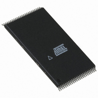
AT49BV322A-70TI Atmel, AT49BV322A-70TI Datasheet - Page 5

AT49BV322A-70TI
Manufacturer Part Number
AT49BV322A-70TI
Description
IC FLASH 32MBIT 70NS 48TSOP
Manufacturer
Atmel
Datasheet
1.AT49BV322A-70TI.pdf
(32 pages)
Specifications of AT49BV322A-70TI
Format - Memory
FLASH
Memory Type
FLASH
Memory Size
32M (4Mx8, 2Mx16)
Speed
70ns
Interface
Parallel
Voltage - Supply
2.65 V ~ 3.6 V
Operating Temperature
-40°C ~ 85°C
Package / Case
48-TSOP
Lead Free Status / RoHS Status
Contains lead / RoHS non-compliant
Available stocks
Company
Part Number
Manufacturer
Quantity
Price
Company:
Part Number:
AT49BV322A-70TI
Manufacturer:
ATMEL
Quantity:
5 530
Company:
Part Number:
AT49BV322A-70TI
Manufacturer:
ATMEL
Quantity:
4 125
Part Number:
AT49BV322A-70TI
Manufacturer:
ATMEL/爱特梅尔
Quantity:
20 000
4.3
4.4
4.4.1
4.4.2
4.5
3308J–FLASH–4/05
Reset
Erasure
Byte/Word Programming
Chip Erase
Sector Erase
microprocessor write timings are used. The address locations used in the command sequences
are not affected by entering the command sequences.
A RESET input pin is provided to ease some system applications. When RESET is at a logic
high level, the device is in its standard operating mode. A low level on the RESET input halts the
present device operation and puts the outputs of the device in a high impedance state. When a
high level is reasserted on the RESET pin, the device returns to the read or standby mode,
depending upon the state of the control inputs.
Before a byte/word can be reprogrammed, it must be erased. The erased state of memory bits is
a logical “1”. The entire device can be erased by using the Chip Erase command or individual
sectors can be erased by using the Sector Erase command.
The entire device can be erased at one time by using the six-byte chip erase software code.
After the chip erase has been initiated, the device will internally time the erase operation so that
no external clocks are required. The maximum time to erase the chip is t
If the sector lockdown has been enabled, the chip erase will not erase the data in the sector that
has been locked out; it will erase only the unprotected sectors. After the chip erase, the device
will return to the read or standby mode.
As an alternative to a full chip erase, the device is organized into 71 sectors (SA0 - SA70) that
can be individually erased. The Sector Erase command is a six-bus cycle operation. The sector
address is latched on the falling WE edge of the sixth cycle while the 30H data input command is
latched on the rising edge of WE. The sector erase starts after the rising edge of WE of the sixth
cycle. The erase operation is internally controlled; it will automatically time to completion. The
maximum time to erase a sector is t
enabled, the sector will erase (from the same Sector Erase command). An attempt to erase a
sector that has been protected will result in the operation terminating immediately.
Once a memory block is erased, it is programmed (to a logical “0”) on a byte-by-byte or on a
word-by-word basis. Programming is accomplished via the internal device command register
and is a four-bus cycle operation. The device will automatically generate the required internal
program pulses.
Any commands written to the chip during the embedded programming cycle will be ignored. If a
hardware reset happens during programming, the data at the location being programmed will be
corrupted. Please note that a data “0” cannot be programmed back to a “1”; only erase opera-
tions can convert “0”s to “1”s. Programming is completed after the specified t
Data Polling feature or the Toggle Bit feature may be used to indicate the end of a program
cycle. If the erase/program status bit is a “1”, the device was not able to verify that the erase or
program operation was performed successfully.
SEC
. When the sector programming lockdown feature is not
AT49BV322A(T)
EC
.
BP
cycle time. The
5


