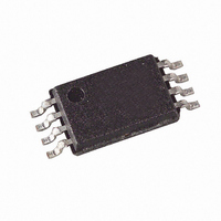
AT24C02A-10TU-1.8 Atmel, AT24C02A-10TU-1.8 Datasheet - Page 8

AT24C02A-10TU-1.8
Manufacturer Part Number
AT24C02A-10TU-1.8
Description
IC EEPROM 2KBIT 400KHZ 8TSSOP
Manufacturer
Atmel
Datasheet
1.AT24C04A-10PU-1.8.pdf
(20 pages)
Specifications of AT24C02A-10TU-1.8
Format - Memory
EEPROMs - Serial
Memory Type
EEPROM
Memory Size
2K (256 x 8)
Speed
100kHz, 400kHz
Interface
I²C, 2-Wire Serial
Voltage - Supply
1.8 V ~ 5.5 V
Operating Temperature
-40°C ~ 85°C
Package / Case
8-TSSOP
Lead Free Status / RoHS Status
Lead free / RoHS Compliant
Available stocks
Company
Part Number
Manufacturer
Quantity
Price
Company:
Part Number:
AT24C02A-10TU-1.8
Manufacturer:
ATMEL
Quantity:
35 000
Device Addressing
Write Operations
8
AT24C02A/04A
The 2K and 4K EEPROM devices require an 8-bit device address word following a start
condition to enable the chip for a read or write operation, as shown in Figure 7.
Figure 7. Device Address
The device address word consists of a mandatory “1”, “0” sequence for the first four
most significant bits as shown. This is common to all the EEPROM devices.
The next three bits are the A2, A1 and A0 device address bits for the 2K EEPROM.
These three bits must compare to their corresponding hardwired input pins.
The 4K EEPROM only uses the A2 and A1 device address bits with the third bit being a
memory page address bit. The two device address bits must compare to their corre-
sponding hardwired input pins. The A0 pin is no-connect.
The eighth bit of the device address is the read/write operation select bit. A read opera-
tion is initiated if this bit is high, and a write operation is initiated if this bit is low.
Upon a compare of the device address, the EEPROM will output a “0”. If a compare is
not made, the chip will return to a standby state.
BYTE WRITE: A write operation requires an 8-bit data word address following the
device address word and acknowledgement. Upon receipt of this address, the EEPROM
will again respond with a “0” and then clock in the first 8-bit data word. Following receipt
of the 8-bit data word, the EEPROM will output a “0” and the addressing device, such as
a microcontroller, must terminate the write sequence with a stop condition. At this time,
the EEPROM enters an internally-timed write cycle, t
inputs are disabled during this write cycle, and the EEPROM will not respond until the
write is complete, see Figure 8 on page 8.
Figure 8. Byte Write
PAGE WRITE: The 2K EEPROM is capable of an 8-byte page write, and the 4K device
is capable of 16-byte page writes.
SDA LINE
S
A
R
T
T
M
S
B
ADDRESS
2K
4K
DEVICE
MSB
1
1
L
S
B
W
W
R
T
E
R
I
/
0
0
A
C
K
M
WORD ADDRESS
S
B
1
1
0
0
A
A
2
2
A
A
1
1
WR
S
B
L
P0
A
, to the nonvolatile memory. All
0
A
C
K
R/W
R/W
LSB
DATA
0976Q–SEEPR–8/05
C
A
K
O
S
T
P


