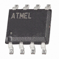
AT45DB041D-SU-2.5 Atmel, AT45DB041D-SU-2.5 Datasheet - Page 46

AT45DB041D-SU-2.5
Manufacturer Part Number
AT45DB041D-SU-2.5
Description
IC FLASH 4MBIT 66MHZ 8SOIC
Manufacturer
Atmel
Specifications of AT45DB041D-SU-2.5
Format - Memory
FLASH
Memory Type
DataFLASH
Memory Size
4M (2048 pages x 264 bytes)
Speed
66MHz
Interface
SPI, RapidS
Voltage - Supply
2.5 V ~ 3.6 V
Operating Temperature
-40°C ~ 85°C
Package / Case
8-SOIC (5.3mm Width), 8-SOP, 8-SOEIAJ
Package
8SOIC EIAJ
Density
4 Mb
Architecture
Sectored
Block Organization
Symmetrical
Typical Operating Supply Voltage
3|3.3 V
Sector Size
64KByte x 8
Timing Type
Synchronous
Interface Type
Serial-SPI
Supply Voltage (max)
3.6 V
Supply Voltage (min)
2.5 V
Maximum Operating Current
15 mA
Mounting Style
SMD/SMT
Organization
64 KB x 8
Current, Input, Leakage
1 μA
Current, Operating
11 mA (Read), 12 mA (Program/Erase)
Current, Output, Leakage
1
Data Retention
20 yrs.
Package Type
EIAJ SOIC
Temperature, Operating
-40 to +85 °C
Time, Access
8 ns
Time, Address Hold
5
Time, Address Setup
5
Time, Fall
6.8 ns
Time, Rise
6.8 ns
Voltage, Input, High
1.75 to 2.52 V
Voltage, Input, Low
0.75 to 1.08 V
Voltage, Output, High
2.5 to 3.4 V
Voltage, Output, Low
0.4 V
Voltage, Supply
2.5 to 3.6 V
Access Time (max)
8ns
Boot Type
Not Required
Address Bus
1b
Operating Supply Voltage (typ)
3/3.3V
Operating Temp Range
-40C to 85C
Program/erase Volt (typ)
2.5 to 3.6V
Sync/async
Synchronous
Operating Temperature Classification
Industrial
Operating Supply Voltage (min)
2.5V
Operating Supply Voltage (max)
3.6V
Supply Current
15mA
Mounting
Surface Mount
Pin Count
8
Lead Free Status / RoHS Status
Lead free / RoHS Compliant
Available stocks
Company
Part Number
Manufacturer
Quantity
Price
Part Number:
AT45DB041D-SU-2.5
Manufacturer:
ATMEL/爱特梅尔
Quantity:
20 000
25. Auto Page Rewrite Flowchart
Figure 25-1. Algorithm for Programming or Reprogramming of the Entire Array Sequentially
Notes:
46
1. This type of algorithm is used for applications in which the entire array is programmed sequentially, filling the array page-by-
2. A page can be written using either a Main Memory Page Program operation or a Buffer Write operation followed by a Buffer
3. The algorithm above shows the programming of a single page. The algorithm will be repeated sequentially for each page
AT45DB041D
page.
to Main Memory Page Program operation.
within the entire array.
MAIN MEMORY PAGE PROGRAM
THROUGH BUFFER
(82H, 85H)
START
END
provide address
and data
MEMORY PAGE PROGRAM
BUFFER TO MAIN
BUFFER WRITE
(84H, 87H)
(83H, 86H)
3595P–DFLASH–09/09


