CY7C1009B-12VC Cypress Semiconductor Corp, CY7C1009B-12VC Datasheet - Page 4
CY7C1009B-12VC
Manufacturer Part Number
CY7C1009B-12VC
Description
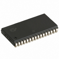
IC SRAM 1MBIT 12NS 32SOJ
Manufacturer
Cypress Semiconductor Corp
Datasheet
1.CY7C1009B-12VC.pdf
(12 pages)
Specifications of CY7C1009B-12VC
Format - Memory
RAM
Memory Type
SRAM - Asynchronous
Memory Size
1M (128K x 8)
Speed
12ns
Interface
Parallel
Voltage - Supply
4.5 V ~ 5.5 V
Operating Temperature
0°C ~ 70°C
Package / Case
32-SOJ
Lead Free Status / RoHS Status
Contains lead / RoHS non-compliant
Other names
428-1000
Available stocks
Company
Part Number
Manufacturer
Quantity
Price
Company:

Part Number:
CY7C1009B-12VC
Manufacturer:
CYPRESS
Quantity:
4 209
Company:
Part Number:
CY7C1009B-12VC
Manufacturer:
CY
Quantity:
5 510
Company:
Part Number:
CY7C1009B-12VCT
Manufacturer:
CYPRESS
Quantity:
372
Part Number:
CY7C1009B-12VCT
Manufacturer:
CYPRESS/赛普拉斯
Quantity:
20 000


Switching Characteristics
Document #: 38-05038 Rev. **
READ CYCLE
t
t
t
t
t
t
t
t
t
t
t
WRITE CYCLE
t
t
t
t
t
t
t
t
t
t
Notes:
Parameter
RC
AA
OHA
ACE
DOE
LZOE
HZOE
LZCE
HZCE
PU
PD
WC
SCE
AW
HA
SA
PWE
SD
HD
LZWE
HZWE
5.
6.
7.
8.
9.
Test conditions assume signal transition time of 3 ns or less, timing reference levels of 1.5V, input pulse levels of 0 to 3.0V, and output loading of the specified
I
t
At any given temperature and voltage condition, t
The internal write time of the memory is defined by the overlap of CE
the transition of any of these signals can terminate the write. The input data set-up and hold timing should be referenced to the leading edge of the signal that terminates the write.
The minimum write cycle time for Write Cycle No. 3 (WE controlled, OE LOW) is the sum of t
OL
HZOE
/I
OH
, t
and 30-pF load capacitance.
HZCE
Read Cycle Time
Address to Data Valid
Data Hold from Address Change
CE
Valid
OE LOW to Data Valid
OE LOW to Low Z
OE HIGH to High Z
CE
CE
CE
Power-Up
CE
Power-Down
Write Cycle Time
CE
Address Set-Up to Write End
Address Hold from Write End
Address Set-Up to Write Start
WE Pulse Width
Data Set-Up to Write End
Data Hold from Write End
WE HIGH to Low Z
WE LOW to High Z
, and t
[8]
1
1
1
1
1
1
LOW to Data Valid, CE
LOW to Low Z, CE
HIGH to High Z, CE
LOW to Power-Up, CE
HIGH to Power-Down, CE
LOW to Write End, CE
HZWE
are specified with a load capacitance of 5 pF as in part (b) of AC Test Loads. Transition is measured 500 mV from steady-state voltage.
[9]
Description
[7]
[6, 7]
[6, 7]
[5]
Over the Operating Range
2
2
HIGH to Low Z
LOW to High Z
2
2
2
HIGH to Write End
HIGH to
HIGH to Data
HZCE
2
LOW to
is less than t
[7]
[6, 7]
LZCE
1
LOW, CE
, t
HZOE
is less than t
2
HIGH, and WE LOW. CE
Min.
12
12
10
10
10
3
0
3
0
0
0
7
0
3
7C1009B-12
7C109B-12
LZOE
, and t
HZWE
HZWE
and t
Max.
12
12
12
6
6
6
6
1
and WE must be LOW and CE
is less than t
SD
.
LZWE
Min.
15
15
12
12
12
3
0
3
0
0
0
8
0
3
for any given device.
7C1009B-15
7C109B-15
2
CY7C1009B
HIGH to initiate a write, and
CY7C109B
Max.
15
15
15
7
7
7
7
Page 4 of 12
Unit
ns
ns
ns
ns
ns
ns
ns
ns
ns
ns
ns
ns
ns
ns
ns
ns
ns
ns
ns
ns
ns
Related parts for CY7C1009B-12VC
Image
Part Number
Description
Manufacturer
Datasheet
Request
R

Part Number:
Description:
IC SRAM 1MBIT 15NS 32SOJ
Manufacturer:
Cypress Semiconductor Corp
Datasheet:
Part Number:
Description:
IC SRAM 1MBIT 20NS 32SOJ
Manufacturer:
Cypress Semiconductor Corp
Datasheet:
Part Number:
Description:
IC SRAM 1MBIT 12NS 32SOJ
Manufacturer:
Cypress Semiconductor Corp
Part Number:
Description:
IC SRAM 1MBIT 20NS 32SOJ
Manufacturer:
Cypress Semiconductor Corp
Part Number:
Description:
IC SRAM 1MBIT 15NS 32SOJ
Manufacturer:
Cypress Semiconductor Corp
Datasheet:

Part Number:
Description:
Manufacturer:
Cypress Semiconductor Corp
Datasheet:
Part Number:
Description:
IC SRAM 1MBIT 15NS 32SOJ
Manufacturer:
Cypress Semiconductor Corp
Datasheet:
Part Number:
Description:
IC SRAM 1MBIT 15NS 32SOJ
Manufacturer:
Cypress Semiconductor Corp
Datasheet:
Part Number:
Description:
Manufacturer:
Cypress Semiconductor Corp
Datasheet:
Part Number:
Description:
Manufacturer:
Cypress Semiconductor Corp
Datasheet: