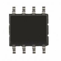
M25P40-VMN6P NUMONYX, M25P40-VMN6P Datasheet - Page 32

M25P40-VMN6P
Manufacturer Part Number
M25P40-VMN6P
Description
IC FLASH 4MBIT 50MHZ 8SOIC
Manufacturer
NUMONYX
Series
Forté™r
Specifications of M25P40-VMN6P
Format - Memory
FLASH
Memory Type
FLASH
Memory Size
4M (512K x 8)
Speed
50MHz
Interface
SPI, 3-Wire Serial
Voltage - Supply
2.3 V ~ 3.6 V
Operating Temperature
-40°C ~ 85°C
Package / Case
8-SOIC (3.9mm Width)
Memory Configuration
512K X 8
Ic Interface Type
Serial, SPI
Clock Frequency
50MHz
Supply Voltage Range
2.3V To 3.6V
Memory Case Style
SOIC
No. Of Pins
8
Lead Free Status / RoHS Status
Lead free / RoHS Compliant
Other names
497-3598
497-3598
497-3598
Available stocks
Company
Part Number
Manufacturer
Quantity
Price
Part Number:
M25P40-VMN6P
Manufacturer:
ST
Quantity:
20 000
Company:
Part Number:
M25P40-VMN6PB
Manufacturer:
ST
Quantity:
102
Part Number:
M25P40-VMN6PB
Manufacturer:
ST
Quantity:
20 000
Part Number:
M25P40-VMN6PBA
Manufacturer:
MICRON
Quantity:
20 000
6.12
32/59
Release from Deep Power-down and Read Electronic
Signature (RES)
To take the device out of Deep Power-down mode, the Release from Deep Power-down and
Read Electronic Signature (RES) instruction must be issued. No other instruction must be
issued while the device is in Deep Power-down mode.
The instruction can also be used to read, on Serial Data output (Q), the old-style 8-bit
electronic signature, whose value for the M25P16 is 14h.
Please note that this is not the same as, or even a subset of, the JEDEC 16-bit electronic
signature that is read by the Read Identifier (RDID) instruction. The old-style electronic
signature is supported for reasons of backward compatibility, only, and should not be used
for new designs. New designs should, instead, make use of the JEDEC 16-bit electronic
signature, and the Read Identifier (RDID) instruction.
Except while an Erase, Program or Write Status Register cycle is in progress, the Release
from Deep Power-down and Read Electronic Signature (RES) instruction always provides
access to the old-style 8-bit electronic signature of the device, and can be applied even if
the Deep Power-down mode has not been entered.
Any Release from Deep Power-down and Read Electronic Signature (RES) instruction while
an Erase, Program or Write Status Register cycle is in progress, is not decoded, and has no
effect on the cycle that is in progress.
The device is first selected by driving Chip Select (S) Low. The instruction code is followed
by 3 dummy bytes, each bit being latched-in on Serial Data input (D) during the rising edge
of Serial Clock (C). Then, the old-style 8-bit electronic signature, stored in the memory, is
shifted out on Serial Data output (Q), each bit being shifted out during the falling edge of
Serial Clock (C).
The instruction sequence is shown in
The Release from Deep Power-down and Read Electronic Signature (RES) instruction is
terminated by driving Chip Select (S) High after the electronic signature has been read at
least once. Sending additional clock cycles on Serial Clock (C), while Chip Select (S) is
driven Low, cause the electronic signature to be output repeatedly.
When Chip Select (S) is driven High, the device is put in the Standby Power mode. If the
device was not previously in the Deep Power-down mode, the transition to the Standby
Power mode is immediate. If the device was previously in the Deep Power-down mode,
though, the transition to the Standby Power mode is delayed by t
must remain High for at least t
waits to be selected, so that it can receive, decode and execute instructions.
RES2
(max). Once in the Standby Power mode, the device
Figure
19.
RES2
, and Chip Select (S)


