CY62128DV30LL-70SXI Cypress Semiconductor Corp, CY62128DV30LL-70SXI Datasheet - Page 3
CY62128DV30LL-70SXI
Manufacturer Part Number
CY62128DV30LL-70SXI
Description
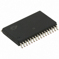
IC SRAM 1MBIT 70NS 32SOIC
Manufacturer
Cypress Semiconductor Corp
Datasheet
1.CY62128DV30LL-70ZI.pdf
(11 pages)
Specifications of CY62128DV30LL-70SXI
Format - Memory
RAM
Memory Type
SRAM
Memory Size
1M (128K x 8)
Speed
70ns
Interface
Parallel
Voltage - Supply
2.2 V ~ 3.6 V
Operating Temperature
-40°C ~ 85°C
Package / Case
32-SOIC (11.30mm Width)
Lead Free Status / RoHS Status
Lead free / RoHS Compliant
Other names
428-1765-5
CY62128DV30LL70SI
CY62128DV30LL70SI
CY62128DV30LL70SI
CY62128DV30LL70SI
Available stocks
Company
Part Number
Manufacturer
Quantity
Price
Company:

Part Number:
CY62128DV30LL-70SXI
Manufacturer:
CYPRESS
Quantity:
329


Document #: 38-05231 Rev. *H
Maximum Ratings
(Above which the useful life may be impaired. For user guide-
lines, not tested.)
Storage Temperature ................................. –65°C to +150°C
Ambient Temperature with
Power Applied............................................. –55°C to +125°C
Supply Voltage to Ground
Potential .......................................................... −0.3V to 3.9V
DC Voltage Applied to Outputs
in High-Z State
DC Electrical Characteristics
Capacitance
Thermal Resistance
V
V
V
V
I
I
I
I
I
C
C
θ
θ
Notes:
Parameter
IX
OZ
CC
SB1
SB2
5. V
6. Full device operation requires linear ramp of V
7. Tested initially and after any design or process changes that may affect these parameters.
JA
JC
Parameter
OH
OL
IH
IL
IN
OUT
IL(min.)
= −2.0V for pulse durations less than 20 ns. V
Parameter
Thermal Resistance
(Junction to Ambient)
Thermal Resistance (Junction to Case)
[5]
Output HIGH Voltage
Output LOW Voltage
Input HIGH Voltage
Input LOW Voltage
Input Leakage Current
Output Leakage Current
V
Current
Automatic CE Power-down
Current − CMOS Inputs
Automatic CE Power-down
Current − CMOS Inputs
[7]
CC
....................................−0.3V to V
Operating Supply
Description
[7]
Description
Input Capacitance
Output Capacitance
(Over the Operating Range)
CC
Description
from 0V to V
2.2 < V
2.7 < V
2.2 < V
2.7 < V
2.2 < V
2.7 < V
2.2 < V
2.7 < V
GND < V
GND < V
f = f
f = 1 MHz
CE
V
f = f
f = 0 (OE, WE,)
CE
V
f = 0, V
IH(max.)
IN
IN
1
1
MAX
MAX
> V
> V
> V
> V
CC
= V
CC(min)
CC
CC
CC
CC
CC
CC
CC
CC
CC
CC
CC
CC
(Address and Data Only),
CC
= 1/t
Still Air, soldered on a 3 x 4.5
inch, two-layer printed circuit
board
+ 0.3V
I
O
CC
=3.6V
< V
< 2.7
< 3.6
< 2.7
< 3.6
< 2.7
< 3.6
< 2.7
< 3.6
− 0.2V, V
− 0.2V or V
< V
+0.75V for pulse durations less than 20 ns
Test Conditions
− 0.2V, CE
− 0.2V, CE
and V
RC
CC
CC
Test Conditions
, Output Disabled
CC
T
V
IN
must be stable at V
A
CC
DC Input Voltage
Output Current into Outputs (LOW)............................. 20 mA
Static Discharge Voltage........................................... > 2001V
(per MIL-STD-883, Method 3015)
Latch-up Current..................................................... > 200 mA
Operating Range
I
I
I
I
V
I
CMOS level
OH
OH
OL
OL
OUT
IN
= 25°C, f = 1 MHz
< 0.2V,
2
2
CC
= V
< 0.2V,
< 0.2V,
< 0.2V,
= 0.1 mA
= 2.1 mA
= −0.1 mA
= −1.0 mA
Test Conditions
= 3.6V,
Industrial
= 0mA,
CC(typ)
Range
CC(min)
L
LL
L
LL
[5]
................................ −0.3V to V
SOIC TSOP I RTSOP STSOP Unit
for 500 µ s.
Temperature (T
69
34
−40°C to +85°C
Min.
−0.3
−0.3
2.0
2.4
1.8
2.2
.
−1
−1
CY62128DV30-55/70
Ambient
93
17
Typ.
0.85
1.5
1.5
1.5
1.5
Max.
5
CY62128DV30
8
8
[4]
A
17
93
)
V
V
CC
CC
2.2V to 3.6V
Max.
0.4
0.4
0.6
0.8
1.5
+1
+1
10
5
4
5
4
+ 0.3
+ 0.3
V
65
15
Page 3 of 11
CC
CC
Unit
[6]
pF
pF
+ 0.3V
Unit
°C/W
°C/W
mA
µA
µA
µA
µA
V
V
V
V
[+] Feedback
Related parts for CY62128DV30LL-70SXI
Image
Part Number
Description
Manufacturer
Datasheet
Request
R

Part Number:
Description:
Manufacturer:
Cypress Semiconductor Corp
Datasheet:
Part Number:
Description:
Manufacturer:
Cypress Semiconductor Corp
Datasheet:
Part Number:
Description:
Manufacturer:
Cypress Semiconductor Corp
Datasheet:
Part Number:
Description:
Manufacturer:
Cypress Semiconductor Corp
Datasheet:
Part Number:
Description:
Manufacturer:
Cypress Semiconductor Corp
Datasheet: