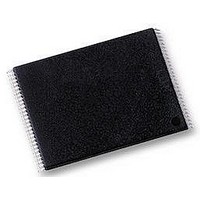
NAND256W3A2BN6E NUMONYX, NAND256W3A2BN6E Datasheet - Page 29

NAND256W3A2BN6E
Manufacturer Part Number
NAND256W3A2BN6E
Description
IC FLASH 256MBIT 48TSOP
Manufacturer
NUMONYX
Datasheet
1.NAND128W3A2BN6E.pdf
(59 pages)
Specifications of NAND256W3A2BN6E
Format - Memory
FLASH
Memory Type
FLASH - Nand
Memory Size
256M (32M x 8)
Interface
Parallel
Voltage - Supply
2.7 V ~ 3.6 V
Operating Temperature
-40°C ~ 85°C
Package / Case
48-TSOP
Access Time
12µs
Supply Voltage Range
1.7V To 1.95V, 2.7V To 3.6V
Memory Case Style
TSOP
No. Of Pins
48
Base Number
256
Block Size
16896Byte
Memory Configuration
32k X 8
Rohs Compliant
Yes
Lead Free Status / RoHS Status
Lead free / RoHS Compliant
Speed
-
Lead Free Status / RoHS Status
Lead free / RoHS Compliant, Lead free / RoHS Compliant
Other names
497-5038
497-5038
497-5038
Available stocks
Company
Part Number
Manufacturer
Quantity
Price
Company:
Part Number:
NAND256W3A2BN6E
Manufacturer:
ST
Quantity:
11 245
Company:
Part Number:
NAND256W3A2BN6E
Manufacturer:
MICRON/EOL43
Quantity:
444
Part Number:
NAND256W3A2BN6E
Manufacturer:
ST
Quantity:
20 000
NAND128-A, NAND256-A
6.5
6.6
6.7
Block erase
Erase operations are done one block at a time. An erase operation sets all of the bits in the
addressed block to ‘1’. All previous data in the block is lost.
An erase operation consists of the following three steps (refer to
operation):
1.
2.
3.
Once the erase operation has completed the status register can be checked for errors.
Figure 16. Block erase operation
Reset
The Reset command resets the command interface and status register. If the Reset
command is issued during any operation, the operation is aborted. If it was a program or
erase operation that was aborted, the contents of the memory locations being modified are
no longer valid as the data is partially programmed or erased.
If the device has already been reset then the new Reset command is not accepted.
The Ready/Busy signal goes Low for t
of t
issued (refer to
Read status register
The device contains a status register which provides information on the current or previous
program or erase operation. the various bits in the status register convey information and
errors on the operation.
the status register is read by issuing the read status register command. the status register
information is present on the output data bus (I/O0-I/O7) on the falling edge of chip enable
or read enable, whichever occurs last. when several memories are connected in a system,
the use of chip enable and read enable signals allows the system to poll each device
separately, even when the ready/busy pins are common-wired. it is not necessary to toggle
the chip enable or read enable signals to update the contents of the status register.
RB
I/O
BLBH4
One bus cycle is required to set up the Block Erase command.
Only two bus cycles are required to input the block address. The first cycle (A0 to A7) is
not required as only addresses A14 to A26 (highest address depends on device
density) are valid, A9 to A13 are ignored. In the last address cycle I/O2 to I/O7 must be
set to V
One bus cycle is required to issue the confirm command to start the P/E/R controller.
Block Erase
Setup Code
depends on the operation that the device was performing when the command was
60h
IL
.
Table 20: AC characteristics for operations
Block Address
Inputs
BLBH4
Confirm
Code
D0h
after the Reset command is issued. The value
(Erase Busy time)
tBLBH3
Busy
for the values.)
Figure 16: Block erase
Read Status Register
70h
Device operations
SR0
ai07593
29/59


