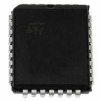
M27C512-45C1 STMicroelectronics, M27C512-45C1 Datasheet - Page 7

M27C512-45C1
Manufacturer Part Number
M27C512-45C1
Description
IC OTP 512KBIT 45NS 32PLCC
Manufacturer
STMicroelectronics
Datasheet
1.M27C512-90B6.pdf
(22 pages)
Specifications of M27C512-45C1
Format - Memory
EPROMs
Memory Type
OTP EPROM
Memory Size
512K (64K x 8)
Speed
45ns
Interface
Parallel
Voltage - Supply
4.5 V ~ 5.5 V
Operating Temperature
0°C ~ 70°C
Package / Case
32-PLCC
Lead Free Status / RoHS Status
Lead free / RoHS Compliant
Available stocks
Company
Part Number
Manufacturer
Quantity
Price
Company:
Part Number:
M27C512-45C1
Manufacturer:
STMicroelectronics
Quantity:
10 000
M27C512
2.5
2.6
Figure 4.
Programming
When delivered (and after each erasure for UV EPROM), all bits of the M27C512 are in the
'1' state. Data is introduced by selectively programming '0's into the desired bit locations.
Although only '0's will be programmed, both '1's and '0's can be present in the data word.
The only way to change a '0' to a '1' is by die exposure to ultraviolet light (UV EPROM). The
M27C512 is in the programming mode when V
The data to be programmed is applied to 8 bits in parallel to the data output pins. The levels
required for the address and data inputs are TTL. V
M27C512 can use PRESTO IIB Programming Algorithm that drastically reduces the
programming time (typically less than 6 seconds). Nevertheless to achieve compatibility with
all programming equipments, PRESTO Programming Algorithm can be used as well.
PRESTO IIB programming algorithm
PRESTO IIB Programming Algorithm allows the whole array to be programmed with a
guaranteed margin, in a typical time of 6.5 seconds. This can be achieved with
STMicroelectronics M27C512 due to several design innovations described in the M27C512
datasheet to improve programming efficiency and to provide adequate margin for reliability.
Before starting the programming the internal MARGIN MODE circuit is set in order to
guarantee that each cell is programmed with enough margin. Then a sequence of 100µs
program pulses are applied to each byte until a correct verify occurs. No overprogram
pulses are applied since the verify in MARGIN MODE provides the necessary margin.
Programming flowchart
YES
NO
FAIL
= 25
++n
V CC = 6.25V, V PP = 12.75V
RESET MARGIN MODE
SET MARGIN MODE
CHECK ALL BYTES
NO
2nd: V CC = 4.2V
E = 100 s Pulse
1st: V CC = 6V
VERIFY
n = 0
Addr
Last
YES
YES
PP
NO
input is at 12.75V and E is pulsed to V
CC
is specified to be 6.25V ± 0.25V. The
++ Addr
AI00738B
Device operation
7/22
IL
.


