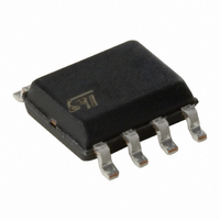
M93S46-WMN6P STMicroelectronics, M93S46-WMN6P Datasheet - Page 23

M93S46-WMN6P
Manufacturer Part Number
M93S46-WMN6P
Description
IC EEPROM 1KBIT 2MHZ 8SOIC
Manufacturer
STMicroelectronics
Datasheet
1.M93S46-WMN6TP.pdf
(34 pages)
Specifications of M93S46-WMN6P
Format - Memory
EEPROMs - Serial
Memory Type
EEPROM
Memory Size
1K (64 x 16)
Speed
2MHz
Interface
Microwire, 3-Wire Serial
Voltage - Supply
2.5 V ~ 5.5 V
Operating Temperature
-40°C ~ 85°C
Package / Case
8-SOIC (3.9mm Width)
Organization
64 K x 16
Interface Type
Microwire
Maximum Clock Frequency
2 MHz
Supply Voltage (max)
5.5 V
Supply Voltage (min)
2.5 V
Maximum Operating Current
2 mA
Maximum Operating Temperature
+ 85 C
Mounting Style
SMD/SMT
Minimum Operating Temperature
- 40 C
Operating Supply Voltage
2.5 V, 5.5 V
Memory Configuration
64 X 16
Clock Frequency
2MHz
Supply Voltage Range
2.5V To 5.5V
Memory Case Style
SOIC
No. Of Pins
8
Rohs Compliant
Yes
Lead Free Status / RoHS Status
Lead free / RoHS Compliant
Other names
497-8596-5
M93S46-WMN6P
M93S46-WMN6P
Available stocks
Company
Part Number
Manufacturer
Quantity
Price
Company:
Part Number:
M93S46-WMN6P
Manufacturer:
STMicroelectronics
Quantity:
1 958
Company:
Part Number:
M93S46-WMN6P
Manufacturer:
ST
Quantity:
6 390
Part Number:
M93S46-WMN6P
Manufacturer:
ST
Quantity:
20 000
Table 17. AC Characteristics (M93Sx6-W, Device Grade 6)
Note: 1. t
Symbol
t
t
t
t
t
t
t
t
t
t
PRVCH
t
t
t
t
t
CLPRX
CHCL
CLCH
t
SLSH
t
WVCH
SLWX
SHCH
DVCH
CHDX
SHQV
CHQL
CHQV
SLCH
CLSH
SLQZ
CLSL
t
f
W
C
2. Chip Select Input (S) must be brought Low for a minimum of tSLSH between consecutive instruction cycles.
3. Current product: identified by Process Identification letter F or M.
4. New product: identified by Process Identification letter W or G.
2
1
1
CHCL
+ t
t
t
t
PRES
t
PREH
t
t
t
t
t
t
t
Alt.
t
t
t
PEH
CSS
t
SKH
CSH
f
PES
SKL
SKS
t
t
PD0
PD1
DIH
DIS
WP
CLCH
SK
CS
SV
DF
1 / f
Clock Frequency
Protect Enable Valid to Clock High
Write Enable Valid to Clock High
Clock Low to Protect Enable Transition
Chip Select Low to Write Enable
Transition
Chip Select Low to Clock High
Chip Select Set-up Time
Chip Select Low to Chip Select High
Clock High Time
Clock Low Time
Data In Set-up Time
Data In Hold Time
Clock Set-up Time (relative to S)
Chip Select Hold Time
Chip Select to Ready/Busy Status
Chip Select Low to Output Hi-Z
Delay to Output Low
Delay to Output Valid
Erase/Write Cycle time
C
.
Test conditions specified in
Parameter
Table 9.
Min.
1000
D.C.
250
250
100
350
250
100
100
100
50
50
0
0
3
and
Max.
Table 6.
400
400
400
200
10
1
3
M93S66, M93S56, M93S46
Min.
D.C.
250
200
200
200
50
50
50
50
50
50
50
0
0
4
Max.
200
100
200
200
2
5
4
MHz
Unit
ms
ns
ns
ns
ns
ns
ns
ns
ns
ns
ns
ns
ns
ns
ns
ns
ns
ns
23/34


