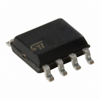
M24512-WMN6P STMicroelectronics, M24512-WMN6P Datasheet - Page 6

M24512-WMN6P
Manufacturer Part Number
M24512-WMN6P
Description
IC EEPROM 512KBIT 400KHZ 8SOIC
Manufacturer
STMicroelectronics
Specifications of M24512-WMN6P
Format - Memory
EEPROMs - Serial
Memory Type
EEPROM
Memory Size
512K (64K x 8)
Speed
400kHz
Interface
I²C, 2-Wire Serial
Voltage - Supply
2.5 V ~ 5.5 V
Operating Temperature
-40°C ~ 85°C
Package / Case
8-SOIC (3.9mm Width)
Memory Configuration
64K X 8
Interface Type
I2C, Serial
Clock Frequency
1MHz
Access Time
500ns
Supply Voltage Range
2.5V To 5.5 V
Memory Case Style
SOIC
No. Of Pins
8
Rohs Compliant
Yes
Lead Free Status / RoHS Status
Lead free / RoHS Compliant
Other names
497-8582-5
M24512-WMN6P
M24512-WMN6P
Available stocks
Company
Part Number
Manufacturer
Quantity
Price
Company:
Part Number:
M24512-WMN6P
Manufacturer:
PANASONIC
Quantity:
60 000
Part Number:
M24512-WMN6P
Manufacturer:
ST
Quantity:
20 000
Description
1
6/41
Description
The M24512-x devices are I
(EEPROM). They are organized as 64 Kb × 8 bits.
The M24512-D also offers an additional page, named the Identification Page (128 bytes)
which can be written and (later) permanently locked in Read-only mode. This Identification
Page offers flexibility in the application board production line, as it can be used to store
unique identification parameters and/or parameters specific to the production line.
The device behaves as a slave in the I
by the serial clock. Read and Write operations are initiated by a Start condition, generated
by the bus master. The Start condition is followed by a device select code and Read/Write
bit (RW) terminated by an acknowledge bit.
When writing data to the memory, the device inserts an acknowledge bit during the 9
time, following the bus master’s 8-bit transmission. When data is read by the bus master, the
bus master acknowledges the receipt of the data byte in the same way. Data transfers are
terminated by a Stop condition after an Ack for Write, and after a NoAck for Read.
Figure 1.
Table 1.
E0, E1, E2
SDA
SCL
WC
V
V
CC
SS
Signal name
Logic diagram
Signal names
2
C-compatible electrically erasable programmable memories
Doc ID 16459 Rev 22
Chip Enable
Serial Data
Serial Clock
Write Control
Supply voltage
Ground
2
C protocol, with all memory operations synchronized
Function
M24512-R, M24512-W, M24512-DR
Inputs
I/O
Input
Input
Direction
th
bit


