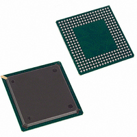
DS3065W-100# Maxim Integrated Products, DS3065W-100# Datasheet - Page 4

DS3065W-100#
Manufacturer Part Number
DS3065W-100#
Description
IC NVSRAM 8MBIT 100NS 256BGA
Manufacturer
Maxim Integrated Products
Datasheet
1.DS3065W-100.pdf
(18 pages)
Specifications of DS3065W-100#
Format - Memory
RAM
Memory Type
NVSRAM (Non-Volatile SRAM)
Memory Size
8M (1M x 8)
Speed
100ns
Interface
Parallel
Voltage - Supply
3 V ~ 3.6 V
Operating Temperature
-40°C ~ 85°C
Package / Case
256-BGA
Lead Free Status / RoHS Status
Lead free / RoHS Compliant
Available stocks
Company
Part Number
Manufacturer
Quantity
Price
AC TEST CONDITIONS
3.3V Single-Piece 8Mb Nonvolatile SRAM
with Clock
DATA RETENTION
(T
4
Note 1:
Note 2:
Note 3:
Note 4:
Note 5:
Note 6:
Note 7:
Note 8:
Note 9:
Note 10: OE = V
Note 11: If the CE or CS low transition occurs simultaneously with or latter than the WE low transition, the output buffers remain in a
Note 12: If the CE or CS high transition occurs prior to or simultaneously with the WE high transition, the output buffers remain in a
Note 13: If WE is low or the WE low transition occurs prior to or simultaneously with the related CE or CS low transition, the output
Expected Data-Retention Time
(Per Charge)
Input Pulse Levels:
Input Pulse Rise and Fall Times:
Input and Output Timing Reference Level:
Output Load:
A
= +25°C.)
_____________________________________________________________________
IRQ/FT and RST are open-drain outputs and cannot source current. External pullup resistors should be connected to these
pins to realize a logic-high level.
These parameters are sampled with a 5pF load and are not 100% tested.
t
the latter of the two related edges going low to the earlier of the two related edges going high.
t
t
t
RTC writes.
In a power-down condition, the voltage on any pin may not exceed the voltage on V
The expected t
user. Minimum expected data-retention time is based upon a maximum of two +230°C convection reflow exposures, fol-
lowed by a fully charged cell. Full charge occurs with the initial application of V
ter is assured by component selection, process control, and design. It is not measured directly during production testing.
WE is high for any read cycle.
high-impedance state during this period.
high-impedance state during this period.
buffers remain in a high-impedance state during this period.
PARAMETER
WP
WR1
WR2
DS
is measured from the earlier of CE or WE going high for SRAM writes, or from the earlier of CS or WE going high for
is specified as the logical AND of CE with WE for SRAM writes, or CS with WE for RTC writes. t
and t
and t
IH
or V
DH1
DH2
IL
are measured from WE going high.
are measured from CE going high for SRAM writes or CS going high for RTC writes.
DR
. If OE = V
is defined as accumulative time in the absence of V
IH
SYMBOL
during write cycle, the output buffers remain in a high-impedance state.
t
DR
V
5ns
1.5V
1 TTL Gate + C
IL
(Notes 7, 8)
= 0.0V, V
IH
= 2.7V
L
(100pF) including scope and jig
CONDITIONS
CC
starting from the time power is first applied by the
CC
for a minimum of 96 hours. This parame-
CC
.
MIN
2
TYP
3
WP
is measured from
MAX
UNITS
years


