PKS606YN Power Integrations, PKS606YN Datasheet - Page 13
PKS606YN
Manufacturer Part Number
PKS606YN
Description
IC OFFLINE SWIT OTP OCP HV TO220
Manufacturer
Power Integrations
Series
PeakSwitch®r
Specifications of PKS606YN
Mfg Application Notes
PeakSwitch Design Guide AppNote
Output Isolation
Isolated
Frequency Range
250 ~ 304kHz
Voltage - Output
700V
Power (watts)
117W
Operating Temperature
-40°C ~ 150°C
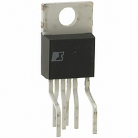
Package / Case
TO-220-7 (Formed Leads), 5 Leads
Output Voltage
12 V
Input / Supply Voltage (max)
265 VAC
Input / Supply Voltage (min)
85 VAC
Duty Cycle (max)
65 %
Switching Frequency
47 KHz
Supply Current
25 uA
Operating Temperature Range
- 40 C to + 150 C
Mounting Style
Through Hole
No. Of Outputs
1
Voltage Regulator Case Style
TO-220
No. Of Pins
7
Base Number
606
Controller Type
PWM
Rohs Compliant
Yes
For Use With
596-1198 - KIT REF DESIGN 36-72W MOTOR DRVR596-1126 - KIT DESIGN ACC PEAKSWITCH FAMILY
Lead Free Status / RoHS Status
Lead free / RoHS Compliant
Other names
596-1122-5
Available stocks
Company
Part Number
Manufacturer
Quantity
Price
Company:

Part Number:
PKS606YN
Manufacturer:
IXYS
Quantity:
5 000
Part Number:
PKS606YN
Manufacturer:
POWER
Quantity:
20 000


DRAIN Voltage .................................. . .............-0.3 V to 700 V
DRAIN Peak Current: ....................... . ..... 2 × I
EN/UV Voltage ....................................................-0.3 V to 9 V
EN/UV Current .................................................... ....... 100 mA
BYPASS Voltage .................................................. - 0.3 V to 9 V
Storage Temperature ......................................-65 °C to 150 °C
Operating Junction Temperature
Lead Temperature
Thermal Impedance: Y/F Package:
Output Frequency
Maximum Duty
Cycle
EN/UV Pin Turn
Off Threshold
Current
EN/UV Pin
Voltage
DRAIN Supply
Current
BYPASS Pin
Charge Current
CONTROL FUNCTIONS
Parameter
(3)
................ . ...................................... 260 °C
(q
(q
P Package:
(q
(q
JA
JC
JA
JC
)
)
) .....................70 °C/W
)
(2)
(5)
(1)
Symbol
..........................................2 °C/W
..................................... 10 °C/W
........................................80 °C/W
DC
f
V
I
I
I
OSC
I
I
CH1
CH2
DIS
S1
S2
EN
MAX
(2)
.................-40 °C to 150 °C
ABSOLUTE MAXIMUM RATINGS
See Figure 4
T
SOURCE = 0 V; T
See Note A, B
EN/UV Open
J
See Note C
See Note C
Switching)
= 25 °C
(MOSFET
T
T
V
V
(Unless Otherwise Specified)
J
J
BP
BP
LIMIT
THERMAL IMPEDANCE
= 25 °C
= 25 °C
= 0 V,
= 4 V,
(3)
; 60 °C/W
(Typical)
I
Conditions
See Figure 18
EN/UV
I
EN/UV
V
S1 Open
EN/UV
= -125 µA
= 25 µA
Peak-Peak Jitter
(5)
(4)
(5)
= 0 V
J
= -40 to 125 °C
Average
Notes:
1. All voltages referenced to SOURCE, T
2. Normally limited by internal circuitry.
3. 1/16 in. from case for 5 seconds.
4. Maximum ratings specified may be applied one at a time,
without causing permanent damage to the product.
5. Peak DRAIN current is allowed while the DRAIN voltage
Notes:
1. Free standing with no heatsink.
2. Measured at the back surface of tab.
3. Soldered to 0.36 sq. in. (232 mm
4. Soldered to 1 sq. in. (645 mm
5. Measured on the SOURCE pin close to plastic interface.
PKS603-604
PKS605-607
PKS603-604
PKS605-607
PKS603
PKS604
PKS605
PKS606
PKS607
Exposure to Absolute Maximum Rating conditions for
extended periods of time may affect product reliability.
is simultaneously less than 400 V. See also Figure 29.
(1,)
-10.0
1160
Min
-350
250
350
460
600
700
950
-7.5
-4.5
-6.5
0.4
1.3
62
2
1175
1430
), 2 oz. (610 g/m
Typ
-240
277
475
570
725
875
-5.0
-6.6
-3.0
-4.5
2
1.0
2.0
16
65
), 2 oz. (610 g/m
PKS603-607
A
= 25 °C.
Max
1050
1400
1700
-200
-2.5
-3.2
-1.5
-2.5
304
600
690
870
1.5
2.7
68
2
2
) copper clad.
) copper clad.
Units
kHz
mA
µA
µA
%
Rev. I 02/07
V
13
Related parts for PKS606YN
Image
Part Number
Description
Manufacturer
Datasheet
Request
R

Part Number:
Description:
SOP-16
Manufacturer:
Power Integrations
Datasheet:
Part Number:
Description:
DIP8
Manufacturer:
Power Integrations
Datasheet:
Part Number:
Description:
TO-263
Manufacturer:
Power Integrations
Datasheet:
Part Number:
Description:
TO-263
Manufacturer:
Power Integrations
Datasheet:
Part Number:
Description:
Manufacturer:
Power Integrations
Datasheet: